Table of Contents
Introduction
This is a long overdue writeup on a topic I presented at this year’s DORS/CLUC conference – another take on a multiboard workflow in KiCad (this one is better than the last one :)). Video of the talk isn’t yet available but the slides are here.
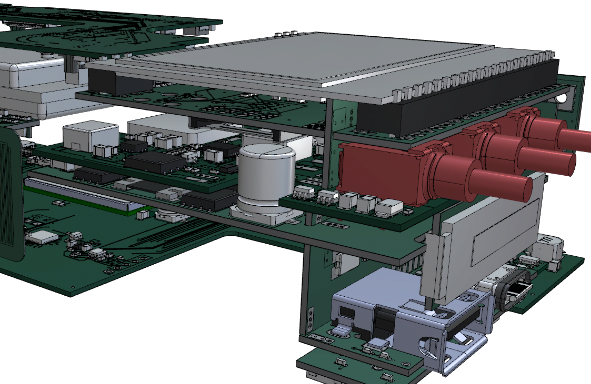
For more than a year now I’ve been working on a quite complex project, spanning across a number of PCBs (22 total in the latest revision!). It’s a commercial project for a client so I can’t go into more details, but I can share my workflow. It’s all, of course, done in KiCad. Due to the project’s nature, the device needs to pack a lot of functionality into relatively small space. Because of that, any available space is used, resulting in PCBs of irregular shapes oriented in all possible ways. Also, the external design and interface/connectors dictate some PCB positions.
KiCad doesn’t have native multi–PCB support but with some external tools it’s relatively easy to do it – do some work, export models and import them in 3D app, check/measure everything, go back to KiCad and iterate.
I’ve already written a post about my old multiboard workflow in KiCad. But that was my own project where I could use a 3D app of my choice and also there were only four boards in a simple arrangement. I used FreeCAD macros to separate a KiCad output into separate PCB objects and position them in space as needed.
But, on a commercial project, when working with a designer, you can’t really ask them to switch to FreeCAD. And they might be using some app which doesn’t support any sort of automation, such as Plasticity (nice tool for some things but automation is definitely not one of them). So, in order to simplify things as much as possible, the idea is to do as little as possible in the 3D app – all translations/rotations should be done in advance.
The whole workflow then consists of the following steps:
- do some work in KiCad
- run a command to extract the board, generate a 3D model and do any 3D transform to get it to the final position
- import it into a 3D app
- check/measure/repeat.
KiCad multiboard basics
Before going into 3D transforms and visualizations, let’s first cover the basics in KiCad. KiKit page about multiboard workflow already covers this in great detail and it’s an excellent starting point.
While not supporting real multiboard workflow, KiCad supports multiple board outlines. After that, KiKit is used to extract outline into a separate KiCad PCB project which can then be used to generate 3D models.
The thing which needs a special care is the separation between boards – each PCB should be fully independent. KiCad 10 brings support for local power nets which can be useful for this.
Connections between boards are done through some sort of connectors, usually either board-to-board headers or mezzanine connectors or some cables (FFC/FPC or some other). It’s also possible to solder boards directly to one another through strategically placed pads, but probably not the best way, especially for use cases with strong vibration.
Unfortunately, there’s no way (that I know of) to specify the relation between two connectors in KiCad. The pinout has to be manually checked and enforced.
Schematic handling
There are two ways to approach the schematic design of a multiboard project. For simple projects it doesn’t really matter but for more complex ones it definitely does. Those two ways are function based and PCB based.
In function based design the whole device is designed normally, as functional units – you have your power supplies, I/O, conditioning, UI and so on. When separating it into multiple PCBs, each of those functional blocks can end up spanning over multiple PCBs. That can end up in having random connector pins all around the schematic projects and it’s not that easy to visualize the signal flow across the boards. Also easy to make a mistake. But someone else checking the schematic will easily figure everything out.
In PCB based design you immediately start with deciding what goes on which PCB and each segment of the schematic project represents a single PCB. This is good when troubleshooting the device since it’s much easier to map a part of the schematic to a part of some board but getting a full picture of the device can be harder. This is the approach the KiKit multiboard page recommends.
I tried both ways and both have pros and cons and the right choice depends on project requirements and personal preference. It would be nice if there would be an option to define the layout in a way to be able to switch between those two views (apparently some advanced EDA tools have that functionality).
3D transforms
STEP is one of the most common interchange file formats for mechanical 3D. Similar to other 3D formats, the geometry is defined relative to a coordinate system, including its position and orientation. That’s why we can perform all of the required transformations in advance, and they will be preserved in the file. The final object can then simply be imported into a 3D app, where it will appear in the proper position and orientation.
So, the first step is to find that proper position:
- export the 3D model of the board from KiCad as a STEP file
- import it into 3D software
- do a series of transforms (rotations and translations) in order to get the board to the required position. Write down that sequence.
For initial manual positioning in FreeCAD the best way is to select the object, open Edit -> Placement, check “Apply incremental changes” and then do the transforms one by one.
To make things simpler it’s recommended to always first do the rotations and then translations. And, while translations are interchangeable, rotations aren’t and the order matters.
With the transform sequence written down, the next step is to have some tool which can do those manipulations. I couldn’t find any command line based option so I wrote my own, using FreeCAD’s Python interface.
step_prepare.py
step_prepare.py is a Python script which exports STEP file from KiCad PCB project and then uses FreeCAD’s command line features in order to process the step file and apply the 3D transforms to it.
❯ ./step_prepare.py --help
usage: step_prepare.py [-h] [-o OUTFILE] [-t TRANSFORM] [--origin ORIGIN] [--skip-kicad-export] [-d] infile

Prepare STEP file from Kicad PCB for mechanical CAD import

positional arguments:
  infile                Input Kicad PCB file

options:
  -h, --help            show this help message and exit
  -o, --outfile OUTFILE
                        Output STEP file
  -t, --transform TRANSFORM
                        Transformations to apply to the STEP file (e.g. "tx100 ty-50 rz90")
  --origin ORIGIN       Origin as "x,y" coordinates, a footprint name (e.g. "pcb_origin", errors out if multiple instances exist) or a reference
                        ("ref:H1"). Defaults to the lowest left corner of the board outline.
  --skip-kicad-export   Skip Kicad STEP export step (assume STEP file already exists)
-d, --detailed-board Use detailed board export options (longer export time)It’s easy to specify the sequence of transforms: just a string of rx|ry|rz|tx|ty|tz with values. For example rx90 ry-90 tx23.4 will first rotate the object around x-axis by 90°, then it will rotate it by -90° around the y-axis and finally move it 23.4mm in the direction of x-axis.
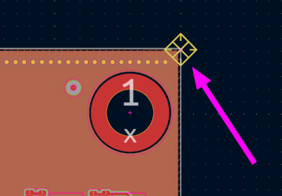
The object’s origin can be defined in multiple ways, either automatically (bottom left point of the board outline) or by specifying a footprint reference or library name with --origin command line argument. I usually create a special footprint with a drawing on some User layer and place it at a convenient place (it needs to be inside the board’s outline). This way, in a multi-PCB project it’s extracted together with the PCB to a separate PCB file from where it can be exported and processed.
The only issue is with colors – all colors are lost and output model is default color. I tried a couple of different ways to retain the colors but wasn’t able to get it done. For now this is fine. For final renders, when everything is set, I manually import and position the models in the file if needed.
Face matching
For some transforms where the board ends up at weird angles around multiple axes, initial manual positioning can be quite hard. That’s why I created a FreeCAD macro which can automate it. Just select the origin face, origin edge and destination face and edge and run the macro and it will print out the sequence of rotations required to get the origin object into the required orientation. It won’t do the translations but those are relatively easy to do manually after the angle is correct.
In FreeCAD:
- go to
Macro -> Macrosin the menu - click
Create, set a name, paste the Python code below - select (in order): origin face, origin edge, destination face, destination Edge
- run the macro, either by selecting it in
Macro -> Macrosdialog and clicking Execute or (if already executed at least once)Macro -> Recent macros
If the object ends up inverted or placed at the wrong angle, play with the FLIP_EDGE and FLIP_NORMAL constants in the macro or try selecting different side of the destination face and edge.
FreeCAD macro code also available at https://gitlab.com/-/snippets/6047539
# -*- coding: utf-8 -*-
# AlignRotation.FCMacro
#
# Computes the rotation that makes a PCB face parallel to (and facing)
# an enclosure face, with a chosen PCB edge parallel to a chosen
# enclosure edge. Prints the result as axis/angle, quaternion and
# yaw/pitch/roll, plus the two-step decomposition (swing + twist).
#
# USAGE
#   1. Click the PCB *mounting* face (the face that must touch the enclosure)
#   2. Ctrl-click a straight edge of the PCB (in-plane direction reference)
#   3. Ctrl-click the enclosure face the PCB mounts onto
#   4. Ctrl-click a straight edge on the enclosure that edge (2) must match
#   5. Run the macro; output appears in the Report view
#      (View > Panels > Report view)
#
# FLAGS
#   APPLY_TO_PCB  True -> actually rotate the PCB object (about the centre of
#                 its mounting face, so it stays put) as a visual preview.
#                 Note: assumes the PCB object sits at document root; if it
#                 lives inside an App::Part / Link, apply the printed rotation
#                 in the appropriate local frame yourself.
#   FLIP_EDGE     True if the result is twisted 180 deg about the face normal
#                 (edge parametrisation direction in STEP is arbitrary).
#   FLIP_NORMAL   True if the PCB ends up facing the wrong way (e.g. you
#                 selected the PCB's top face instead of the mounting face).

import math
import FreeCAD as App
import FreeCADGui as Gui
import Part

APPLY_TO_PCB = True
FLIP_EDGE    = False
FLIP_NORMAL  = True

# --------------------------------------------------------------- helpers

def _picks():
    """(object, subname, sub-shape in GLOBAL coordinates), in selection order.

    Part.getShape with needSubElement=True applies all placements along the
    path, including App::Link / App::Part containers.
    """
    out = []
    for sel in Gui.Selection.getSelectionEx('', 0):
        for sub in sel.SubElementNames:
            shp = Part.getShape(sel.Object, sub, needSubElement=True)
            out.append((sel.Object, sub, shp))
    return out

def _parent_shape(obj, sub):
    """Whole shape (global coords) of the object owning the sub-element."""
    parts = sub.split('.')
    if parts and parts[-1][:4] in ('Face', 'Edge', 'Vert'):
        sub = '.'.join(parts[:-1])
        if sub:
            sub += '.'
    try:
        return Part.getShape(obj, sub)
    except Exception:
        return None

def _valid_uv(face):
    """A (u, v) pair that actually lies on the face (avoids holes)."""
    u0, u1, v0, v1 = face.ParameterRange
    for i in range(1, 8):
        for j in range(1, 8):
            u = u0 + (u1 - u0) * i / 8.0
            v = v0 + (v1 - v0) * j / 8.0
            try:
                if face.isPartOfDomain(u, v):
                    return u, v
            except Exception:
                break
    return 0.5 * (u0 + u1), 0.5 * (v0 + v1)

def outward_normal(face, whole):
    """Unit normal of a planar face, verified to point OUT of the material.

    STEP faces are frequently 'Reversed', and normalAt()'s handling of that
    has varied between versions -- so instead of trusting flags we probe a
    point along the normal and check it is outside the parent solid.
    """
    if face.findPlane() is None:
        raise ValueError("selected face is not planar")
    u, v = _valid_uv(face)
    n = face.normalAt(u, v)
    n.normalize()
    if whole is not None and whole.Volume > 1e-9:
        p = face.valueAt(u, v)
        d = max(whole.BoundBox.DiagonalLength * 1e-4, 1e-2)
        try:
            if whole.isInside(p + n * d, 1e-7, False):
                n = n.negative()
        except Exception:
            pass
    return n

def in_plane_dir(edge, n):
    """Unit direction of the reference edge, projected into the face plane."""
    t = edge.tangentAt(0.5 * (edge.FirstParameter + edge.LastParameter))
    t.normalize()
    t = t - n * t.dot(n)
    if t.Length < 1e-6:
        raise ValueError("reference edge is (nearly) perpendicular to the face plane")
    t.normalize()
    return t

def decompose_xyz(R):
    """Angles (ax, ay, az) in degrees such that R = Rz(az) * Ry(ay) * Rx(ax),
    i.e. applied to the model as: rotate about GLOBAL X by ax, then GLOBAL Y
    by ay, then GLOBAL Z by az (extrinsic X-Y-Z order).

    Extracted from the rotation matrix columns; handles the gimbal case
    ay = +/-90 deg (there ax/az are not unique -- az is set to 0).
    """
    cx = R.multVec(App.Vector(1, 0, 0))   # matrix column X
    cy = R.multVec(App.Vector(0, 1, 0))   # matrix column Y
    cz = R.multVec(App.Vector(0, 0, 1))   # matrix column Z
    m20 = cx.z                            # = -sin(ay)
    if m20 < -0.999999999:                # ay = +90 deg, gimbal
        ay, az = 90.0, 0.0
        ax = math.degrees(math.atan2(cy.x, cz.x))
    elif m20 > 0.999999999:               # ay = -90 deg, gimbal
        ay, az = -90.0, 0.0
        ax = math.degrees(math.atan2(-cy.x, -cz.x))
    else:
        ay = math.degrees(math.asin(-m20))
        ax = math.degrees(math.atan2(cy.z, cz.z))
        az = math.degrees(math.atan2(cx.y, cx.x))
    return ax, ay, az

def fmt(v):
    return "({:.6f}, {:.6f}, {:.6f})".format(v.x, v.y, v.z)

def say(msg=""):
    App.Console.PrintMessage(msg + "\n")

# ------------------------------------------------------------------ main

picks = _picks()
ok = (len(picks) == 4
      and picks[0][2].ShapeType == 'Face' and picks[1][2].ShapeType == 'Edge'
      and picks[2][2].ShapeType == 'Face' and picks[3][2].ShapeType == 'Edge')
if not ok:
    raise RuntimeError(
        "Select exactly 4 things, in this order (Ctrl-click):\n"
        "  1) PCB mounting face   2) PCB reference edge\n"
        "  3) enclosure face      4) enclosure reference edge")

pcb_obj, pcb_sub, f_src = picks[0]
e_src = picks[1][2]
enc_obj, enc_sub, f_tgt = picks[2]
e_tgt = picks[3][2]

if not isinstance(e_src.Curve, Part.Line):
    say("warning : PCB reference edge is not straight; using mid-point tangent")
if not isinstance(e_tgt.Curve, Part.Line):
    say("warning : enclosure reference edge is not straight; using mid-point tangent")

n_src = outward_normal(f_src, _parent_shape(pcb_obj, pcb_sub))
n_tgt = outward_normal(f_tgt, _parent_shape(enc_obj, enc_sub))

n_dst = n_tgt.negative()            # mounting face must LOOK AT the enclosure face
if FLIP_NORMAL:
    n_dst = n_dst.negative()

t_src = in_plane_dir(e_src, n_src)
t_dst = in_plane_dir(e_tgt, n_tgt)
if FLIP_EDGE:
    t_dst = t_dst.negative()

# Step 1 -- "swing": minimal rotation taking the PCB normal onto the target
R1 = App.Rotation(n_src, n_dst)

# Step 2 -- "twist": rotate about the target normal to line the edges up
t_mid = R1.multVec(t_src)
twist = math.degrees(math.atan2(n_dst.dot(t_mid.cross(t_dst)), t_mid.dot(t_dst)))
R2 = App.Rotation(n_dst, twist)

R = R2.multiply(R1)                 # a.multiply(b) applies b FIRST, then a

# --------------------------------------------------------------- report

err_n = math.degrees(R.multVec(n_src).getAngle(n_dst))
err_t = math.degrees(R.multVec(t_src).getAngle(t_dst))
yaw, pitch, roll = R.toEuler()

say("=== AlignRotation ===")
say("PCB     : {}  [{}]".format(pcb_obj.Label, pcb_sub))
say("target  : {}  [{}]".format(enc_obj.Label, enc_sub))
say("normal  : pcb {}  ->  goal {}".format(fmt(n_src), fmt(n_dst)))
say("edge    : pcb {}  ->  goal {}".format(fmt(t_src), fmt(t_dst)))
say()
say("step 1  : swing {:.6f} deg about {}".format(math.degrees(R1.Angle), fmt(R1.Axis)))
say("step 2  : twist {:.6f} deg about {} (target normal)".format(twist, fmt(R2.Axis)))
say()
say("combined rotation:")
say("  axis/angle : {:.6f} deg about {}".format(math.degrees(R.Angle), fmt(R.Axis)))
say("  quaternion : ({:.9f}, {:.9f}, {:.9f}, {:.9f})".format(*R.Q))
say("  Placement dialog (yaw/pitch/roll): Z={:.6f}  Y={:.6f}  X={:.6f}"
    .format(yaw, pitch, roll))
say()

# ---- rotation sequence for export into another 3D tool -----------------
ax, ay, az = decompose_xyz(R)
Rx = App.Rotation(App.Vector(1, 0, 0), ax)
Ry = App.Rotation(App.Vector(0, 1, 0), ay)
Rz = App.Rotation(App.Vector(0, 0, 1), az)
Rseq = Rz.multiply(Ry).multiply(Rx)          # Rx applied first, Rz last
resid = math.degrees(Rseq.inverted().multiply(R).Angle)

say("EXPORT SEQUENCE  (about the FIXED GLOBAL axes, in this order):")
say("  1) rotX  {:+.6f} deg".format(ax))
say("  2) rotY  {:+.6f} deg".format(ay))
say("  3) rotZ  {:+.6f} deg".format(az))
say("  reconstruction residual: {:.2e} deg (should be ~0)".format(resid))
say("  note: if the target tool rotates about LOCAL axes that follow the")
say("        object, apply the SAME angles in reverse order: rotZ -> rotY -> rotX")
say()
say("  python : obj.Placement.Rotation = App.Rotation({:.9f}, {:.9f}, {:.9f})"
    .format(yaw, pitch, roll))
say()
say("check   : normal error {:.2e} deg, edge error {:.2e} deg".format(err_n, err_t))
say("hint    : twisted 180deg? set FLIP_EDGE=True."
    "  Board flipped/inside the wall? set FLIP_NORMAL=True.")

if APPLY_TO_PCB:
    c = f_src.CenterOfMass                      # global centre of mounting face
    delta = App.Placement(App.Vector(0, 0, 0), R, c)   # rotate about c
    pcb_obj.Placement = delta.multiply(pcb_obj.Placement)
    App.ActiveDocument.recompute()
    say("applied : PCB rotated about its mounting-face centre {}".format(fmt(c)))
Putting it all together
I like to glue it all together with a shell script which does all of the mentioned steps: extracts the board to a separate project (I like to put it into 3d_exchange dir), fixes library paths (I keep all of my custom symbols/footprints/3D models in a lib/{symbols|footprints|3D}), exports 3D model and does the required 3D manipulations. The resulting STEP file can then be directly imported into the 3D software.
So, if I have my main project where I used KiKit annotation to annotate some PCB with PcbMain then, after I run ./extract_board.sh PcbMain I’ll get 3d_exchange/PcbMain/PcbMain_transformed.step which I can directly import into 3D software of choice.
The basic skeleton of my extract_board.sh script is available below. Only changes required are to set the SOURCE_PCB and define the BOARDS list.
extract_board.sh code also available at https://gitlab.com/-/snippets/6047553
#!/bin/bash

set -x

SOURCE_PCB=input_pcb.kicad_pcb
OUTDIR=3d_exchange

# ref             transform   — add new boards here, one line each
BOARDS=(
  "PcbMain    tx-27 ty-20"
  "PcbSensor  rx90 ty21.6 tx2"
  "PcbPower   rx90 rz-90 tx21.6 ty-2"
)

extract_board() {
    local BOARDREF=$1 TRANSFORM=$2

    mkdir -p "${OUTDIR}/${BOARDREF}"

    # A stale ~<ref>.kicad_pro.lck makes KiCad's settings manager silently skip writing
    # <ref>.kicad_pro. kikit then json.loads the leftover 0-byte file and aborts with
    # "Expecting value: line 1 column 1", so an interrupted run poisons every rerun.
    rm -f "${OUTDIR}/${BOARDREF}/~${BOARDREF}.kicad_pro.lck"
    for f in "${OUTDIR}/${BOARDREF}/${BOARDREF}".kicad_{pro,prl}; do
        [ -e "$f" ] && [ ! -s "$f" ] && rm -f "$f"
    done

    # extract the board
    kikit separate --source 'annotation; tolerance: 2mm; ref: '"${BOARDREF}" ${SOURCE_PCB} "${OUTDIR}/${BOARDREF}/${BOARDREF}.kicad_pcb"
    if [ $? -ne 0 ]; then
        echo "Error: Failed to extract board ${BOARDREF}"
        return 1
    fi

    # fix the library path - local/custom 3D models are placed in ./lib/3D_models but the
    # separated board is extracted to $OUTDIR
    sed -i -r 's/\$\{KIPRJMOD\}\/lib\//\$\{KIPRJMOD\}\/..\/..\/lib\//g' "${OUTDIR}/${BOARDREF}/${BOARDREF}.kicad_pcb"

    #time ./step_prepare.py "${OUTDIR}/${BOARDREF}/${BOARDREF}.kicad_pcb" --detailed-board --origin pcb_origin -t "${TRANSFORM}"
    time ./step_prepare.py "${OUTDIR}/${BOARDREF}/${BOARDREF}.kicad_pcb" --origin pcb_origin -t "${TRANSFORM}"
}

if [ $# -eq 0 ]; then
    echo "usage: $0 list|all|<board> [board ...]"
    exit 1
fi

if [ "$1" == "list" ]; then
    for entry in "${BOARDS[@]}"; do
        read -r name _ <<< "$entry"
        echo "$name"
    done
    exit 0
fi

REFS=("$@")
if [ "$1" == "all" ]; then
    REFS=()
    for entry in "${BOARDS[@]}"; do
        read -r name _ <<< "$entry"
        REFS+=("$name")
    done
fi

RC=0
for ref in "${REFS[@]}"; do
    TRANSFORM=""
    found=0
    for entry in "${BOARDS[@]}"; do
        read -r name rest <<< "$entry"
        if [ "$name" == "$ref" ]; then
            TRANSFORM=$rest
            found=1
            break
        fi
    done

    if [ $found -eq 0 ]; then
        echo "Warning: No transform defined for board ${ref}"
    fi

    extract_board "$ref" "$TRANSFORM" || RC=1
done

exit $RC