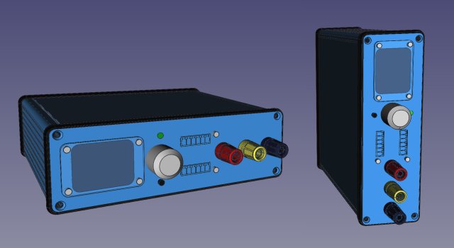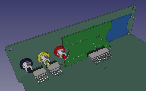
As part of the work on JellyfishOPP I had to decide on what sort of enclosure will I use and figure out the whole layout of the device.
This article will cover the basics of using FreeCAD together with KiCad to (more or less) easily visualize the whole multi PCB project.
This layout isn't particularly complex (four interconnected PCBs in total) but getting all of the connectors and cutouts aligned properly can be a bit tricky and FreeCAD can help a lot with that.
JellyfishOPP is an open source, open hardware, programmable power supply and a measurement device. The main page containing the description and links to all of the development updates can be found here: https://hyperglitch.com/jellyfish.
Development of the device is funded by NLnet through the NGI0 Entrust fund. Learn more at the NLnet project page.
Table of Contents
Enclosure
Based on the requirements I previously specified and required connectors/controls, the width of the device couldn't be less than 150mm to be able to comfotably use the device and in order to follow some standard practices (i.e. 19.05mm distance between banana connectors). Device height needs to be at least 35mm to fit the display module. The layout doesn't specify the depth of the device, but looking around for standard extruded aluminum enclosures I found out that some of the standard sizes are 160x100 and 160x160mm. Due to the sheer number of the components on the main PCB I decided to go with the 160x160mm size - a bit bigger than I would like, but it should give me enough space to fit everything.
By looking around I found this Hammond enclosure. It fits the requirements and even comes in multiple colors: clear, black, blue and red. It's not cheap (i.e. around 35€ for clear/black and slightly more for blue/red) but it's much cheaper than a similar enclosure from Fischer and it's available from multiple distributors. Due to the relatively standard size it's also quite possible that there are other manufacturers that make similar enclosures with lower price.
For the first prototype I went with the blue version.
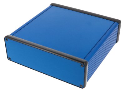
Nice thing about this enclosure is that it comes with plastic bezels. My idea is to make front and back panels as PCBs so bezels will hide the PCB edges and make the device look more professional. Another nice thing is that the 3D model of the enclodure is available on the Hammond website which makes this task much easier.
Multi-PCB project? In KiCad?
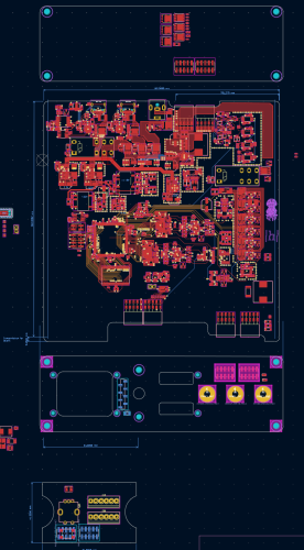
KiCad doesn't officially support multi-PCB project (yet). It will, though, allow (and visualize) to draw multiple PCBs in the same project (just put multiple closed shapes on the Edge.Cuts layer) and with the use of the amazing KiKit it is possible to extract each PCB to a separate project when needed for production.
A few notes on the KiKit. It's a super useful tool used for various PCB production related tasks. It can be used to (among other things): extract one PCB from a multi-PCB KiCad project, create a panelized PCB and export the production files (Gerber, drill files, position files, BOM) for some fab houses.
I usually add a simple bash script to all of my KiCad projects which will prepare the production files. For example, in the JellyfishOPP project I have a prepare_everything.sh script which will, based on the selected PCB, extract it from the main file and optionally prepare the production files.
Although the KiKit can be used with annotations inside the kicad_pcb file, I usually prefer to specify everything from the command line. For example, to extract the main PCB for the JellyfishOPP the command would be:
kikit separate --source 'rectangle; tlx: 60mm; tly: 75mm; brx: 240mm; bry: 250mm' JellyfishOPP.kicad_pcb production/{revision}/jellyfish_main.kicad_pcbSo, what do we want?
After deciding on the enclosure (which pretty much fixed the main PCB dimensions) I started to play with the device layout in FreeCAD. I started with importing the enclosure, drawing the display module, adding all of the connectors and controls and fiddling around to find out the best placement for everything.
One of the ideas that came is that it would be nice to use the device in both the horizontal and vertical orientation. This means that it's important for the connectors/controls to be centered on the panel.
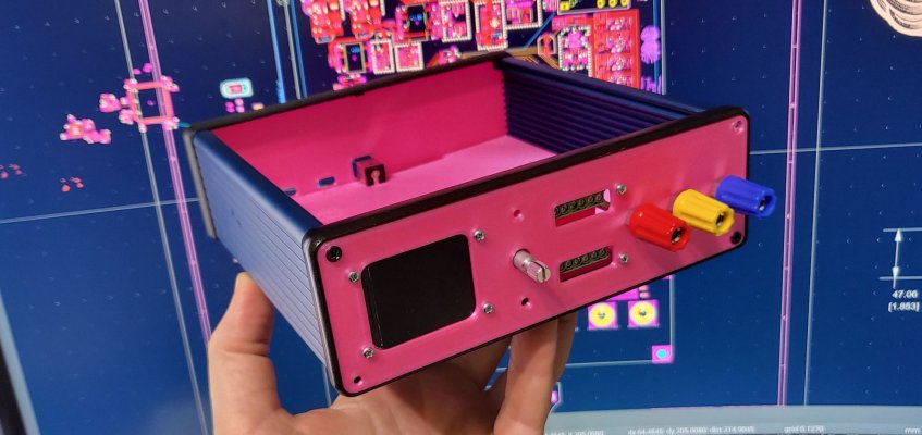
After a bit of playing around I came to this layout:
Initial idea was to use the two-row terminal block (which is quite rarely used and hence quite expensive) for the GPIO pins but there was no way to align it nicely with the encoder. Also, adding the LED+button next to the encoder would be quite hard.
Due to that I decided to go with two separate terminal blocks and add a small PCB which will hold the terminal blocks, encoder and the LED+button. This allows for a much cleaner and more flexible layout with the cost of one additional PCB.
And I needed a way to visualize this to properly align all of the cutouts and mounting holes.
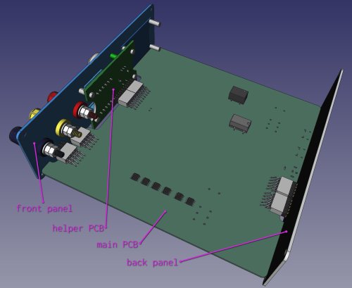
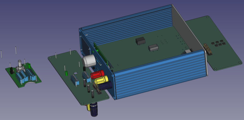
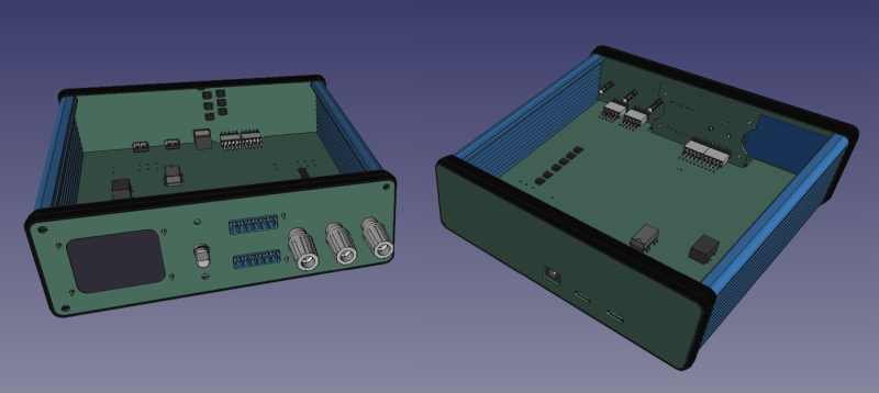
So, here's the complete idea:
- back plate will have cutouts for the power connectors. It will also contain the power stage so that the heatsink can be added and to minimize the heat spreading to the main PCB. It's onnected to the main PCB with two 2x5 2.54mm pitch connectors (based on testing and power requirements this can be aluminum based PCB, maybe with additional small fan if needed)
- front plate will have the cutouts for the display, encoder, LED+button and the terminal blocks. It will contain the main banana connectors and the display module will be directly mounted on it. It's connected to the main PCB via two 2x5 2.54mm pitch connectors (one for the banana connectors and one for the display).
- small PCB will hold the terminal blocks, encoder, LED and the button. It will be mounted on the front plate and connected to the main PCB via two 2x5 2.54mm pitch connectors (one for the encoder, LED and button and the other for the terminal blocks).
- everything should be as simple as possible to assemble and disassemble
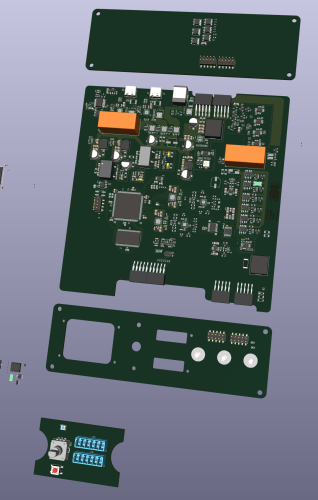
Playing with the header connectors and cutouts I came to this layout. Just the main PCB is the real PCB, the rest are just placeholders to visualize the whole thing:
Next step is to design all of the surrounding PCBs and to properly align all of the connectors and cutouts.
The workflow
The workflow is quite simple:
- design the PCBs in KiCad
- export the 3D model of the project
- import the 3D model in FreeCAD
- align the placeholder PCBs and components with the 3D model of the PCB
- check/measure the differences, update the KiCad project and repeat until everything is aligned properly
This is the slower approach which gives immediate results in 3D (personally I find it easier to match the connectors this way). Another approach is to export the graphics/technical drawing from FreeCAD and import the image into KiCad for alignment (Place -> Add Reference Image) - I used this approach for the connector/display cutouts but it can be tricky to match the scaling properly.
Note on 3D file formats
KiCad can export PCB (with components) in STEP and VRML formats (also, each component can have 3D model specified in both of those formats). While VRML is by default quite nicer looking it has some downsides. Most important one is the bug in FreeCAD where the document can become corrupted if saved with VRML model imported (seems to be fixed in 0.21.2 but I need to test it further). On the plus side, STEP format keeps all of the components as separate objects so it's easy to move them around (and this is exactly what we need as we need to position the front/back panel PCBs in the right position).
When exporting the STEP file from KiCad (File -> Export -> STEP...) there's an option to also export tracks, pads and vias but it can create quite big file and will take a lot of time to import.
FreeCAD crash course
FreeCAD has a bit of a learning curve and has a lot of features. I won't go into any of the details - just the basics needed import different models and move them around the space.
UI Layout
There are few main parts of the FreeCAD UI:
- the 3D space
- the tree view which shows all of the objects in the scene
- the property view which shows the properties of the selected object
- the toolbar with the workbench selection and the tools.
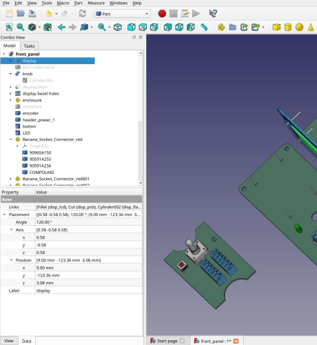
Here's how the default UI looks like with the "Part" workbench selected:
One thing I always do is to enable the "Auto expand" option in the property view (by right-clicking on the property view and selecting "Auto expand"). This way all of the properties are always visible.
Navigation
There are a few ways to navigate the 3D space in FreeCAD. Those can be selected by right-clicking the 3D space and selecting the navigation style. I personally prefer the "Touchpad" style as it seems the simplest to me - hold Shift and move the mouse for panning, hold Alt and move the mouse for rotation. Mouse wheel zooms in and out.
Importing and adding simple models
To import a model into FreeCAD use the File -> Import... option. FreeCAD supports a lot of formats (including STEP and VRML). After importing the model it will be added to the tree view and will be visible in the 3D space.
For testing the UIs and doing mockups, some simple shapes can be very useful - cubes, cylinders, etc. Those can be added by selecting the "Part" workbench and selecting the desired shape from the toolbar.
By clicking the part in the tree view (or in the 3D space) the properties will be shown in the property view. Here it's possible to change the size, position and rotation of the object.
Positioning
Simple positioning can be done directly in the property view by changing the x, y and z values of the Position. Also it's easy to add rotation around the single axis.
For more complex positioning the Edit -> Placement option can be used. This will open a dialog where it's possible to change the position and rotation of the object in a more intuitive way including the incremental changes and the ability to set the center for rotation (including the object's center of mass).
It's important to be aware of the view - the default view (ortographic) might look weird to those unfamiliar with 3D tools. The view can be changed between the ortographic and perspective by selecting the desired view in the View menu.
The perspective view is more natural as it does perspective correction but it's not good for positioning objects as it can be hard to align them properly. The ortographic view is better for that as it doesn't have perspective correction and it's easier to align objects.
Group transform
When some number of objects, be it separate objects or components inside other objects, need to be moved/transformed together (such as the whole front panel with the controls), it's possible to group them together. This can be done by selecting all of them (Ctrl+clicking in the tree view or 3D space) and then right-clicking and selecting Link actions -> Make link group -> Simple group (I don't really know what other options do but this one seems to work for me). This will create a new object in the tree view which can be moved/rotated as a single object (but the sub-objects can also be transformed separately which is sometimes needed).
Measurements
The Part workbench contains a tool for measuring distances between points, lines and planes - yellow tape measure icon in the toolbar. After clicking it the selections window will appear in the sidebar instead of tree/property view. There it indicates the current state and gives the options to clear measurements and close the dialog. Note that some interactions/property editing are limited while the measurement tool is active so it's good to close it when not needed.
Bonus feature: macros and scripting
One of the pretty cool things about FreeCAD is that it's fully scriptable in Python. And it's really easy! For years I was avoiding it for some reason but now I see how easily any repetitive task can be automated. Cool thing is that, after you enable the Python console (View -> Panels -> Python console) any action in the UI will be shown as a Python command in the console. This way it's easy to learn how to do things in Python. Additionally, it's really simple to create a macro - open Macro -> Macro Recording, do the actions you want to record and stop the recording with Macro -> Stop macro recording. Note that this will record all of the actions (like all the steps while moving some object) so it's good idea to open the macro (in the Macro -> Macros menu) and clean up all of the extra steps.
Let's do the actual work
So, here's exactly how I did the work:
- I have all PCBs (main PCB, front and back panel, helper PCB for terminal blocks and encoder) in the same file. When I export the PCB as step file and import it into FreeCAD I am able to separately move each of the PCBs and components around.
-
In order to minimize the unnecessary repetitive work, after importing the PCBs in FreeCAD I re-positioned the enclosure and all other components to match the position of the main PCB. This way I can easily delete and re-import the PCB after making changes without the need to re-position everything.
-
I made the transformation groups for the front panel, back panel and the helper PCB containing the placeholder parts and all of the components/connectors. Then I positioned those groups to match the positions of the imported PCBs. Other way is also possible (described in step 5) but for me, for most of the positioning this seems simpler and step 5 is for fine tuning.
-
Now the task is to measure or estimate the required offset for each component, update the KiCad PCB and repeat until everything is aligned properly.
-
After everything is aligned more or less properly I can make the transform groups with the parts of the imported PCBs and position them to match the enclosure to check if everything fits properly.
For the last step I wrote a Python script/macro which selects PCB sub-elements based on y-coordinate (to separate the PCBs), creates link groups and positions them in the right place. This way I can easily re-import the PCBs and position them properly with one click. Here's the script:
# -*- coding: utf-8 -*-

import FreeCAD

doc_name = 'front_panel'    # actual file name
pcb_obj = 'JellyfishOPP_1'  # name of the imported PCB object in the object tree

doc = App.getDocument(doc_name)
pcbs = doc.getObject(pcb_obj)

link_group_prefix = '__lg__'    # name for the link groups in the tree view

# define pcbs based on the y-coordinate range (figure it out after importing the pcb step file)
sections = {
    'back': (45, 110),
    'main': (-130, 45),
    'front': (-190, -130),
    'ui': (-240, -190)
}

objects = {
    'back': [],
    'main': [],
    'front': [],
    'ui': []
}

# put each object in its section based on the min/mas Y coordinate of the bounding box
for p in pcbs.Group:
    bb = p.Shape.BoundBox
    for s in ('back', 'main', 'front', 'ui'):
        if bb.YMin>=sections[s][0] and bb.YMax<=sections[s][1]:
            objects[s].append(p)

# make link groups for each section
for sec in ('back', 'main', 'front', 'ui'):
    lg = link_group_prefix + sec
    # remove link group if exists
    try:
        doc.removeObject(lg)
    except:
        pass
    doc.addObject('App::LinkGroup', lg) # create new link group
    __objs__ = []

    for p in objects[sec]:
        # append to the list and hide
        __objs__.append(doc.getObject(p.Name))
        doc.getObject(p.Name).ViewObject.Visibility=False

    doc.getObject(lg).setLink(__objs__)
    del __objs__

# numbers based on the positioning in the GUI
doc.getObject('__lg__front').Placement = App.Placement(App.Vector(0.5,-126,-141.3),App.Rotation(App.Vector(1,0,0),-90))
doc.getObject('__lg__ui').Placement = App.Placement(App.Vector(1.56,-115.78,233.94),App.Rotation(App.Vector(1,0,0),90))
doc.getObject('__lg__back').Placement = App.Placement(App.Vector(0.55,40.8,-59.3),App.Rotation(App.Vector(1,0,0),90))