Table of Contents
Introduction
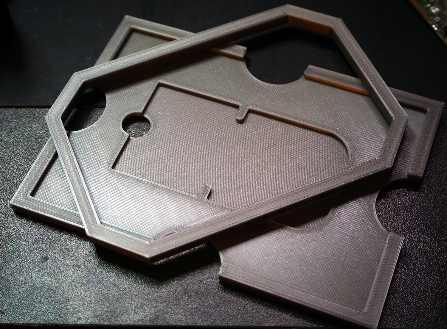
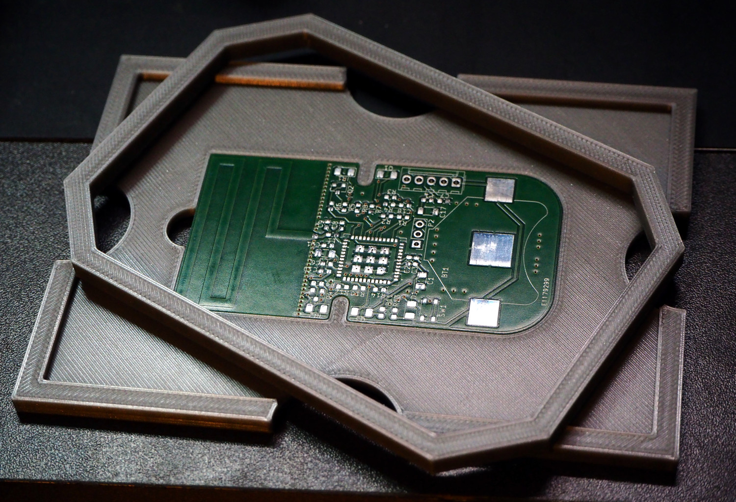
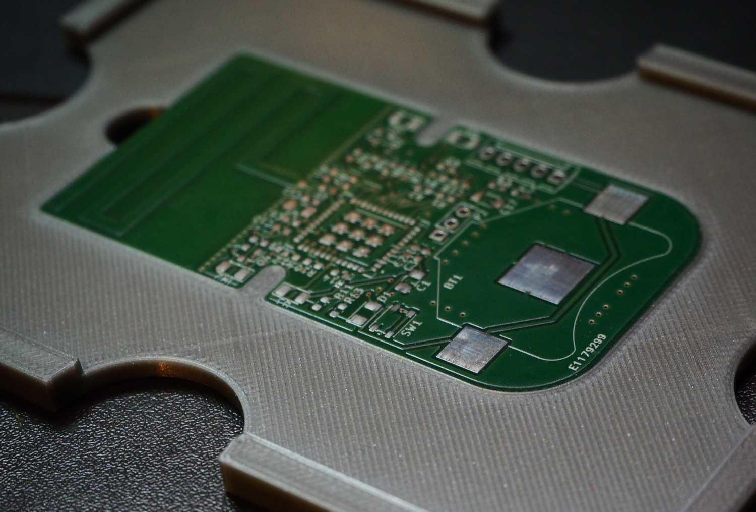
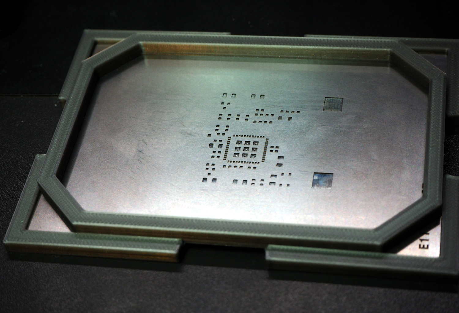
When prototyping, I usually order PCBs together with small, frameless stencils (usually from Eurocircuits if I'm in a rush and from seeed or JLC when I can wait a few weeks). Previously, for applying solder paste to the PCB, I've used different arrangements of old PCBs taped to my desk and the stencil taped over all of it and all of it was quite cumbersome. For a recent project I manually designed the printed part which holds the PCB and stencil in place and it proved to be of great help. Since I have few boards to assemble and test in the upcoming weeks I decided to automate the whole process.
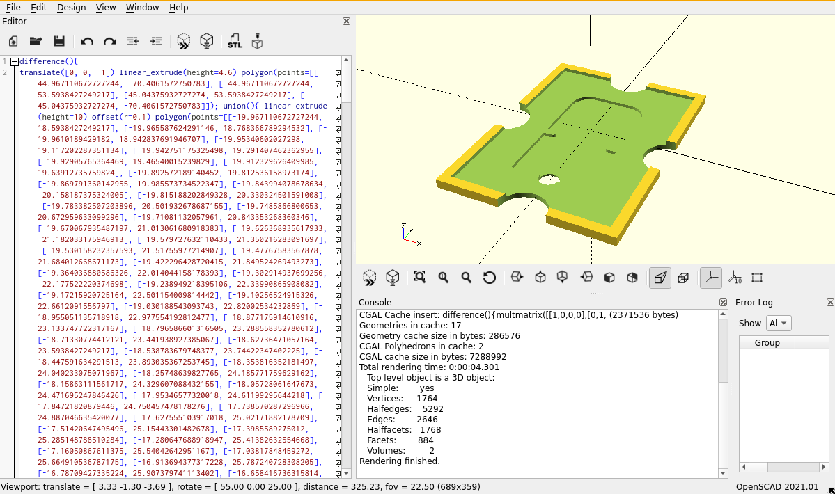
Stencilframer is a Python script which takes the KiCAD PCB or Gerber file (outline, Edge_Cuts layer) as an input and, using OpenSCAD in the background, produces STL/AMF mesh which can be sliced and 3D printed. It can also export PNG image or the actual OpenSCAD code used for the model (for further adjustments). Only dependencies for running it are Python and OpenSCAD
UPDATE 2023/10/29: Stencilframer code updated to support KiCAD 6.0 and newer (I've also completely rewritten the parsing of the KiCAD PCB file, so it should be more robust now)
Video
How it works
Stencilframer script takes the KiCAD PCB or gerber (outline/Edge_Cuts layer, supported extensions are .kicad_pcb, .gbr, .gm1) file and extracts the shapes from the Edge.Cuts layer (i.e. board outline). Then it converts it into OpenSCAD polygon (list of vertices) which is extruded to get the shape of the PCB (arcs are replaced by a series of short straight lines). Based on the PCB and the stencil margins (margin between PCB edge and stencil edge can be adjusted for each side) it also creates and extrudes the shape for the stencil. A small offset (0.1mm default) is added to both shapes. Those two shapes are subtracted from the base element and some cutouts are added to simplify taking out the PCB and stencil.
In addition, a separate frame/cover can be generated (by using the --frame argument) which is placed on top of the stencil to keep it in place.
When the OpenSCAD code is generated, the OpenSCAD executable is called in order to generate the output files. The format of the output file is set based on the output filename extension.
If the PCB has some cutouts (i.e. more than one closed shape on the Edge.Cuts layer) the script will recognize more than one shape in the file and desired shape can be selected using the --shape argument.
Usage
The script allows most of the parameters to be set from command line
> ./stencilframer.py --help
usage: stencilframer.py [-h] [-l MARGIN_LEFT] [-r MARGIN_RIGHT] [-t MARGIN_TOP] [-b MARGIN_BOTTOM] [-m] [-p PCB_THICKNESS] [-s SHAPE]
                        [-f] [-k] [-o OFFSET] [--stencil-offset STENCIL_OFFSET] [--openscad OPENSCAD]
                        infile outfile

positional arguments:
  infile                path to KiCad PCB or gerber file (.kicad_pcb, .gbr, .gm1)
  outfile               path to output file (extension can be .stl, .amf, .png, .pdf, .scad)

optional arguments:
  -h, --help            show this help message and exit
  -l MARGIN_LEFT, --margin-left MARGIN_LEFT
                        Left margin (mm) (default: 20)
  -r MARGIN_RIGHT, --margin-right MARGIN_RIGHT
                        Right margin (mm) (default: 20)
  -t MARGIN_TOP, --margin-top MARGIN_TOP
                        Top margin (mm) (default: 20)
  -b MARGIN_BOTTOM, --margin-bottom MARGIN_BOTTOM
                        Bottom margin (mm) (default: 20)
  -m, --mirror          Mirror the PCB (to get the bottom side up) (default: False)
  -p PCB_THICKNESS, --pcb-thickness PCB_THICKNESS
                        Thickness of the PCB (mm) (default: 1.6)
  -s SHAPE, --shape SHAPE
                        Index of the desired shape from input file (default: 0)
  -f, --frame           Generate stencil holding frame instead of stencil frame (default: False)
  -k, --skip-holes      Don't add holes for easy removal in the fixture (default: False)
  -o OFFSET, --offset OFFSET
                        Offset between the PCB/stencil and frame edge (mm) (default: 0.1)
  --stencil-offset STENCIL_OFFSET
                        Offset between the stencil and frame edge (mm). If not specified, the --offset is used (default: None)
  --openscad OPENSCAD   Path to OpenSCAD executable (default: openscad)
Alternative use
Since the holder has a slot in which the PCB fits so perfectly, by skipping holes for easy removal and adjusting margins, it can be turned into nice frame for showing off your PCBs :)
> stencilframer.py  -p 1.6 radiona4093.kicad_pcb -k -l 5 -r 5 -t 5 -b 5 out.stl
OpenSCAD version 2021.01
Found 1 closed shapes inside the file
CGAL Cache insert: union(){linear_extrude(height=10,center= (1242960 bytes)
CGAL Cache insert: difference(){multmatrix([[1,0,0,0],[0,1, (643536 bytes)
Geometries in cache: 10
Geometry cache size in bytes: 79224
CGAL Polyhedrons in cache: 2
CGAL cache size in bytes: 1886496
Total rendering time: 0:00:00.491
   Top level object is a 3D object:
   Simple:        yes
   Vertices:      478
   Halfedges:    1434
   Edges:         717
   Halffacets:    486
   Facets:        243
   Volumes:         2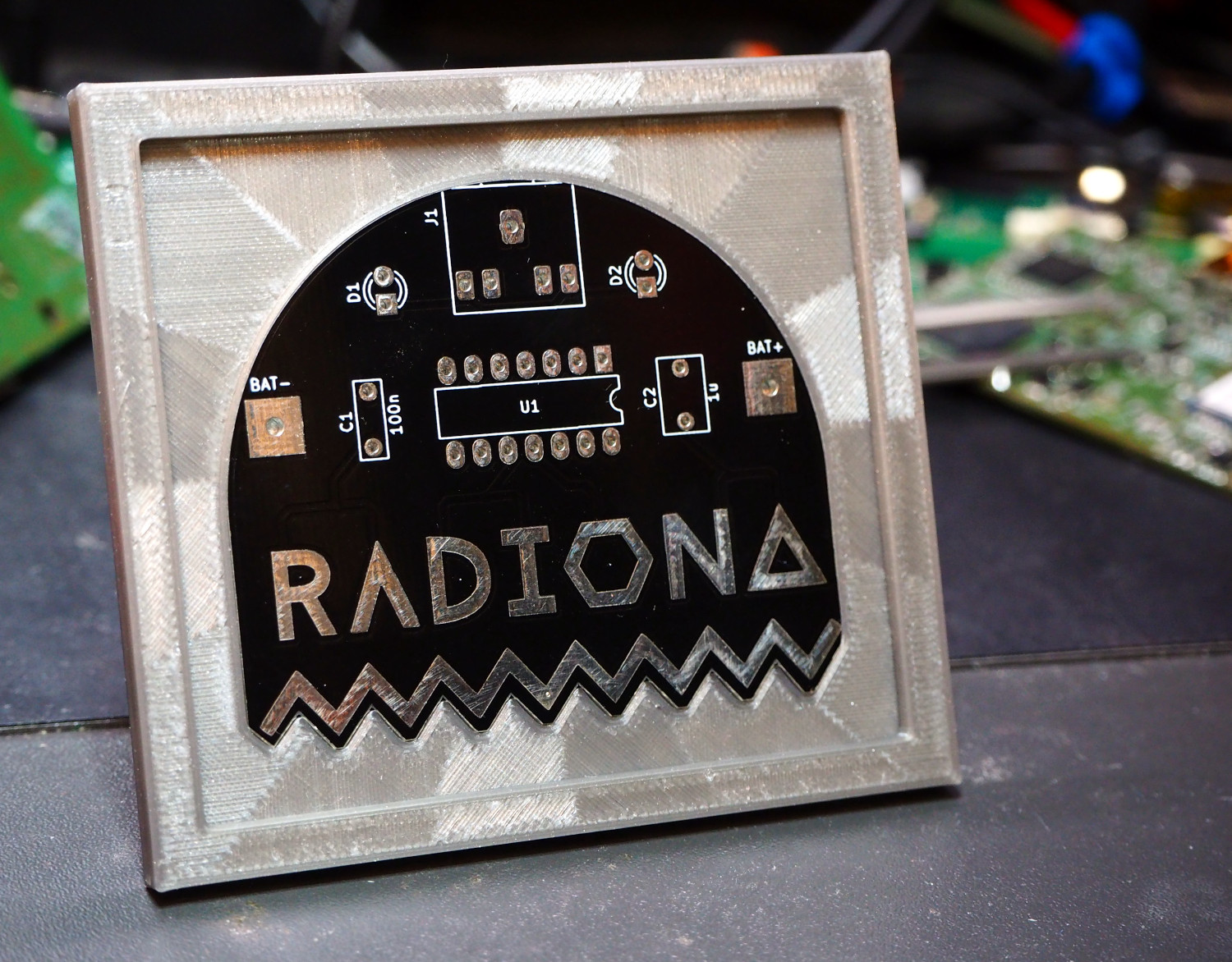
Code
Code is available at https://bitbucket.org/igor_b/stencilframer/