
About
A couple of months ago I had a need for two specialized tools to help with PCB design. I was working on a complex multi-PCB project where I needed to be able to allow two engineers to work on separate boards inside the same KiCad PCB file and then be able to check the differences and merge them. And after the design was done I needed to make a complex panel consisting of different PCBs (due to the number of different PCBs it wasn’t viable to order and assemble separate PCBs for the prototypes). Since the required tools weren’t available or weren’t supporting everything I needed, I decided to build them myself.
Note: both projects were built with the help of LLM coding tools.
deltaKi (ΔKi)
ΔKi is a visual diff+merge tool for KiCad PCB files. It supports loading different versions of local files as well as loading the two different revisions of a file from a (public) git repository (supported are GitLab, GitHub and Codeberg, including self-hosted versions). The tool can also be used as a handy PCB visualizer as it supports most of the features of KiCad 10. The PCB rendering engine is built from scratch and isn’t based on any of the existing projects.
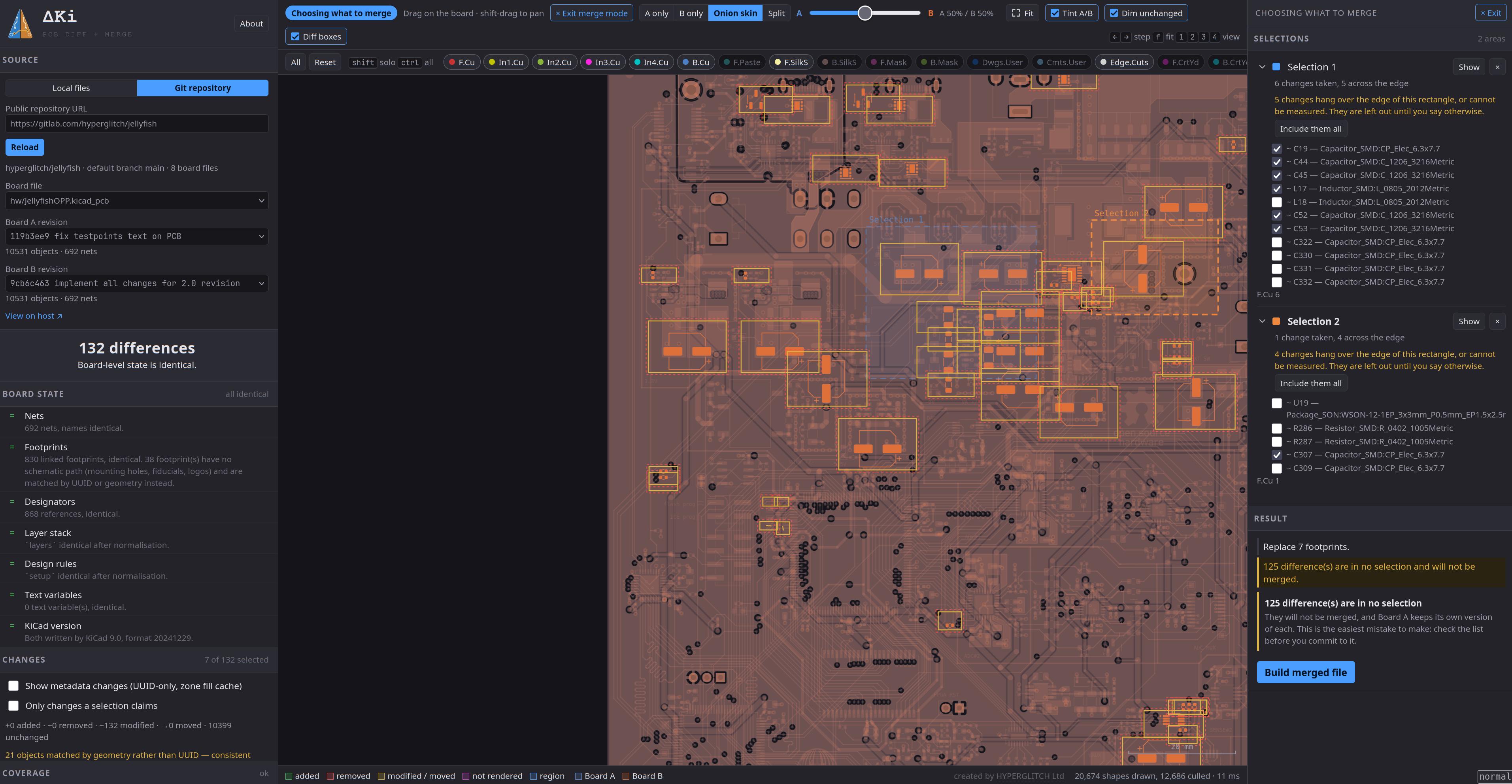
This is a pure browser based tool – nothing is uploaded to the server and the page doesn’t make any network connections (unless a git repository is used in which case it needs to be able to fetch the remote files).
The hosted version of the tool is available at https://deltaki.hyperglitch.com and the source code is available at https://gitlab.com/hyperglitch/deltaki.
Screen is split into 2-3 vertical sections (third one appears when merging). Left sidebar shows the file loading options together with board statistics. It allows the user to either load two separate files or switch to “Git repository” tab and provide the repository URL (note: it won’t work on self hosted servers without proper CORS headers set). It also shows the full list of differences between the board revisions. The middle part shows the rendered PCB with options to enable/disable layers and control the diff options. Clicking the “Start merging” button in the left sidebar opens the right sidebar and allows the user to make selections on the board. All of the differences inside different selected areas are listed. The user can then sepect which changes to merge and click “Build merged file” which will then merge the differences to the A board and allow the user to save the resulting board as a kicad_pcb file.
IMPORTANT DISCLAIMER: I built this tool for personal use. It is provided AS-IS, meaning I’m not taking any responsibility for bugs in the tool or damaged/lost files. Use it at your own risk and make backups.
I’ve used it and fixed the bugs I found. There probably are others. It worked for me well enough to publish it, which doesn’t necessarily mean it will work for you.
sigmaKi (ΣKi)
While KiKit is amazing tool for board separation and panelization which I often use, for non-standard uses (such as different PCBs in the panel) it’s not so straightforward to use as it requires direct Python scripting.
At first I wanted just a CLI tool which takes the panel specification and builds the full KiCad panel based on it. The specification file specifies all parts of the panel: source files, board outlines, frame, rails, tabs. I first built that and it worked great. It is available at https://gitlab.com/hyperglitch/sigmaki. It’s built on top of KiKit and it’s using those primitives in order to build the panel.
However, after building it I realized that for more complex panels it still takes a lot of time to build the spec files. And got the idea to build the GUI tool for it.
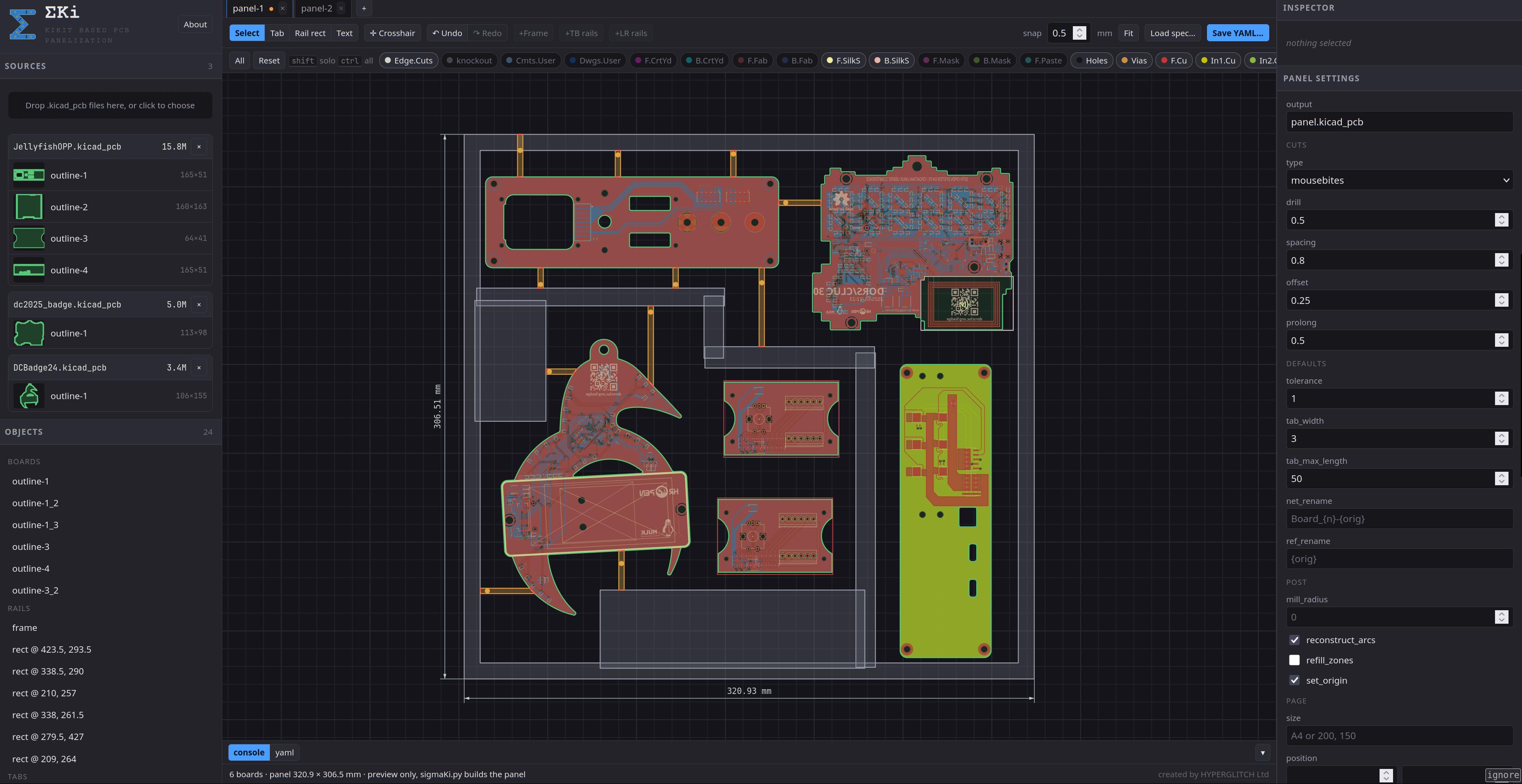
The GUI is similar to deltaKi – same design style and layout. It’s also using the same PCB rendering engine.
The left sidebar allows loading multiple KiCad PCB files. After loading it lists all of the board outlines it found in each file. The outlines then can be dragged onto the main part and placed as desired. The middle part is the editor. Everything can be dragged around and clicked. The right sidebar shows the properties of the selected object and panel’s properties in general. The toolbar above the editor contains editing tools. Editor also has tabs so multiple panels can be built at the same time from the same source files.
The tool also allows the loading of the existing spec file (“Load spec…” in the top right corner of the editor). After loading the spec file it will ask for the required KiCad PCB files in order to display the panel.
The GUI editor is a pure browser based tool – nothing is uploaded to the server and the page doesn’t make any network connections.
After building the panel, the spec file can be downloaded using “Save YAML…” button. The generated YAML file can then be used locally with the sigmaKi.py script. The actual panel building, especially for bigger panels can take some time and a lot of RAM/CPU and that’s the reason the second step isn’t provided online. It would also require actually uploading the files to the server which pulls in the privacy concerns.
❯ ~/repos/sigmaKi/sigmaKi.py  --help
usage: sigmaKi.py [-h] [-o OUTPUT] [--base-dir DIR] [--check] [-q]
                  [--progress | --no-progress]
                  [spec]

sigmaKi.py -- Build a KiCad panel from a declarative YAML/JSON spec using
KiKit.

positional arguments:
  spec                 YAML or JSON panel specification

options:
  -h, --help           show this help message and exit
  -o, --output OUTPUT  override output .kicad_pcb path
  --base-dir DIR       resolve board files and output against DIR (default: the
                       spec file's own directory)
  --check              validate the spec and print its geometry, then exit
                       without rendering
  -q, --quiet          do not print the placement summary
  --progress           show the progress bar even when stderr is redirected
  --no-progress        never show the progress bar (default: shown on a
                       terminal)
The simplest is to have all required KiCad PCB files and the spec in the same directory. In that case the panel build is done simply using /path/to/sigmaKi.py spec.yaml --output panel.kicad_pcb. Before building, especially for bigger panels, a check can be done with /path/to/sigmaKi.py spec.yaml --check.
IMPORTANT DISCLAIMER: as with deltaKi, I built this tool for personal use. It is provided AS-IS, meaning I’m not taking any responsibility for bugs in the tool or damaged/lost files. Use it at your own risk and make backups. Always check the generated files before sending them to production.
I already used this tool for building quite important/expensive panels and it worked great. Your mileage may vary.
The hosted version of the GUI tool is available at https://sigmaki.hyperglitch.com and the source code is available at https://gitlab.com/hyperglitch/sigmaki-web.
The sigmaKi Python script which does the actual panelization is available at https://gitlab.com/hyperglitch/sigmaki