There are a lot of things to cover in this update, from some administrative things, over the firmware itself and supporting apps, to the hardware and things which still need some work. This update took a long time to complete, mostly due to some personal things getting in the way, so let's start.
JellyfishOPP is an open source, open hardware, programmable power supply and measurement device. The main page containing the description and links to all of the development updates can be found here: https://hyperglitch.com/jellyfish.
Development of the device is funded by NLnet through the NGI0 Entrust fund. Learn more at the NLnet project page.
Table of contents
Table of Contents
Misc things
There are three things here which I'd like to mention.
First one is that the second revision of the device is officially certified as open source hardware by OSHWA under the UID HR00019.
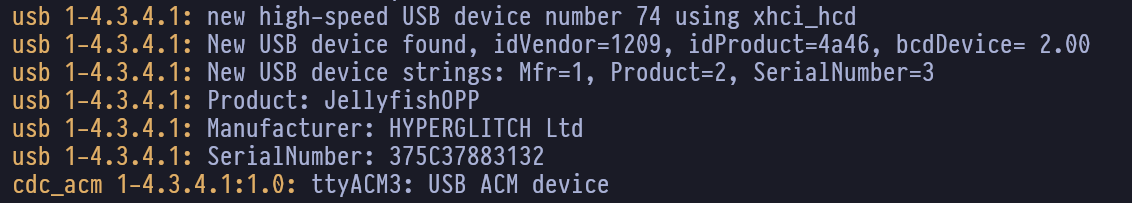
In addition to that, JellyfishOPP also got the USB official VID/PID code from pid.codes. The VID is 0x1209 and the PID is 0x4A46 (spelling "JF" in ASCII). This means that, when connected to the host device, it can properly "introduce" itself :)
The third thing is a logo for the project. I've been playing with various versions of this logo for the last year or so but in the end awesome Lucijana from Studio Utopia did the final tweaks both to the jellyfish image and the typography and took it to a new level (this actually happened quite a long time ago but I haven't mentioned it in any of other updates yet).

USB
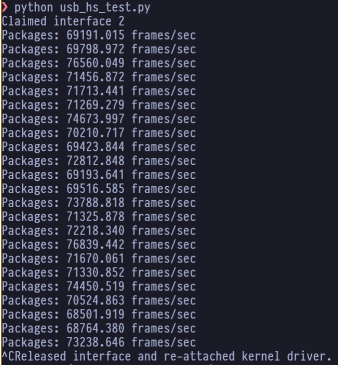
One of the main features (besides the actual measurement capabilities) is to be able to send the data to the host device. For that, two data channels are needed - the slow one for control and a fast one for actual data transfer. Because of that, JellyfishOPP is a composite USB high speed device and it appears as a both CDC (serial) device for easy control without the need for any special apps and as a bulk USB device (raw data) for fast data streaming, requiring an app to parse the data (theoreticaly up to 480MBps but realisticaly much less). This was slightly difficut to implement as the CubeMX doesn't support the configuration of the composite USB device. Due to that, the whole USB stack together with the device descriptors had to be added manually without involving the CubeMX. In the end I had some help with implementing the USB descriptors and that part took some time but was successfuly done. The sw/usb_hs_test.py script can be used to test the data transfer.
SCPI
SCPI (Standard Commands for Programmable Instruments, pronounced "skippy") is a standard protocol used by a lot of test & measurement equipment to communicate with the host device. It supports various data types and physical layers (serial, ethernet, ...). The serial port of the JellyfishOPP speaks SCPI which allows it to be controlled from many host applications, such as Envox EEZ Studio or just a regular serial terminal.
The image below shows querying and sending commands to the JellyfishOPP from the EEZ Studio.
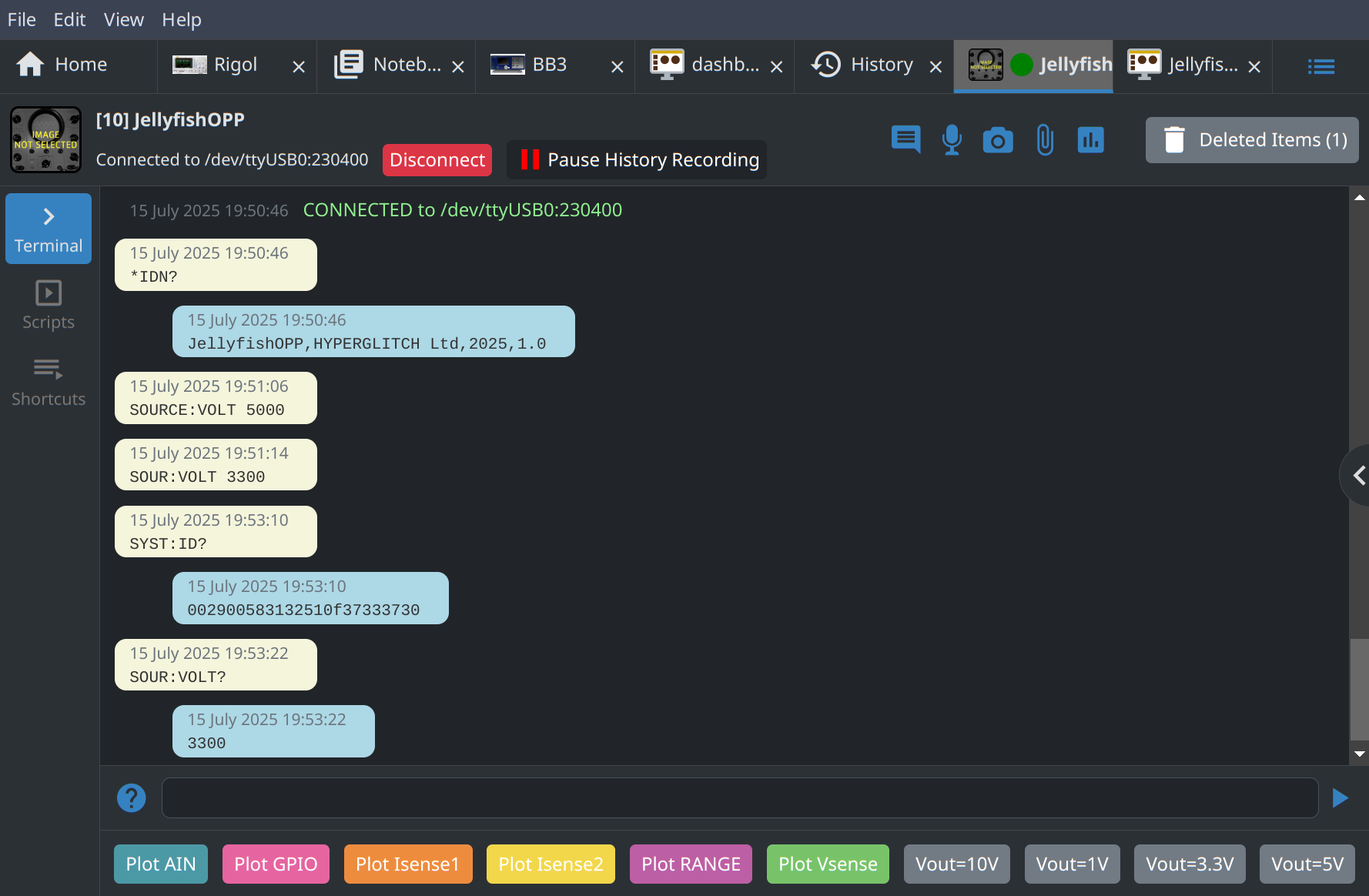
SCPI parser library v2 by Jan Breuer was used to implement the SCPI. The implemented commands allow controlling all of the functionality, from setting the voltage, current limits and measurement range to controlling the AUX supply and the overall routing. The host scripts (calibration, battery profiling) are based on these commands in order to configure the device.
Currently implemented commands are:
IDN?- get the device infoSYSTem:ID?- get device UIDSOURce?,SOURce,SOURce:TOGgle- query or enable/disable main outputSOURce:VOLTage?,SOURce:VOLTage- query or set the output voltage (in mV)SOURce:DAC- set the raw DAC code for main outputSOURce:CURRent,SOURce:CURRent?,SOURce:CURRent:POSitive,SOURce:CURRent:POSitive?,SOURce:CURRent:NEGative,SOURce:CURRent:NEGative?- query or set the hardware current limitAUX?,AUX,AUX:TOGgle- query or enable/disable the AUX outputAUX:VOLTage?,AUX:VOLTage- query or set the AUX voltageAUX:CURRent?,AUX:CURRent- query or set the AUX current limit (software based)MEASure:RANGe?,MEASure:RANGe- query or set the measurement range. Values areR0,R1,R2,R3,R4,R5,AUTO,OFFMEASure:ISENSE1?,MEASure:ISENSE2?,MEASure:VSENSE?,MEASure:GPIO?,MEASure:AUX:VOLTage?,MEASure:AUX:CURRent?- get current dataROUTE:ISO?,ROUTE:ISO- query or enable/disable USB isolationROUTE:EXTin?,ROUTE:EXTin- query or enable/disable external inputROUTE:OUTput?,ROUTE:OUTput- query or enable/disable main output
Auto range switching
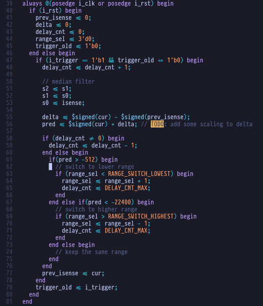
In each ADC sampling cycle, after getting the raw ADC codes, the FPGA checks the values and runs the automatic range switching algorithm. The initial version I wrote was very simple - if the currently measured value is outside the ADC code range defined with two threshold values, it switches to higher or lower range. That wasn't the best, especialy with faster current changes and it also had a lot of oscillations immediately after the range is changed.
The problem here is that, when the FPGA gets the ADC code, that code is actually a value from the previous cycle. And a delay in any control loop, if not handled properly, can easily cause the oscillations.
The improved version includes a simple linear prediction algorithm which first applies a three-point median filter to the current measurement to filter out possible noise/outliers and then check the difference between the current and previous sample. Based on that difference it switches the range in time. It also doesn't allow a range switch immediately after another one and it requires some number of cycles (4-8 seem to be a good value) to pass before the next switch in order to prevent the oscillations.
Python module
The libjellyfishopp Python module is used for fetching and parsing the data stream from the JellyfishOPP. It spawns a background process which continuously receives the USB data, splits it into frames and parses the frames, applying the calibration to it (each frame contains one measurement from 4 ADC channels, GPIO status and current measurement range). The JellyfishOPP sends the raw data received from FPGA as adding the parsing to the device takes too much resources (the device only parses one frame from each buffer and averages the values over 100 samples to use it for the display). This parsing turned to be quite intensive for pure Python and had to be quite optimized. I managed to get the parsing throughput up to around 400-500k frames (samples) per second with Python by using numpy array and memoryview (significant improvement from the initial value of under 200k frames per second by using naive approach). This currently works as the device still samples and sends the data at under 100ksps. Once the sampling rate goes higher I'll probably have to rewrite the module in C or C++.
Calibration
Each device needs to be calibrated in order to get the correct relation between the ADC/DAC codes and the actual voltages. One approach is to precisely measure all of the resistors which are affecting those relations which can be a tedious job. Another one is to consider the whole part as a black box with an input and an output and model the relations. Since the JellyfishOPP can give the variable voltage and can precisely measure both the current and voltage, the calibration requires just a multimeter.
There are a few things which need to be calibrated:
- conversion from the set voltage in volts to the DAC code
- coversion from the ADC voltage measurement to the actual voltage
- coversion from the ADC current measurement to the actual current for each measurement range
Calibration is done by using the jf_calibrate.py script. It accepts the option to calibrate either voltage (both the DAC and ADC) or current. The script is using the libjellyfishopp Python library for fetching the data and SCPI interface for the control.
For the voltage calibration, the script sets the raw DAC code to set the output voltage, measures the ADC voltage (16 bit value) and asks the user the actual voltage measured by using a voltmeter. Four voltage values are set and for each one some number of samples are averaged. Weighted linear fit, which in addition to averaged values also takes in account the measurement uncertainty, is used to estimate the slope and intercept values (we know it's a linear relation based on the hardware design).
For current calibration, the ampere meter is connected directly to the main output and the current is measured. The ampere meter has very low resistance but it has the current sense resistor in series so by applying voltage to the output some range of values can be measured. The script goes through each measurement range where it first sets the different voltages on the output to find the minimum and maximum values where the measurement is inside the ADC range. It then sets the three voltage values (all inside the ADC range) and asks the user for actual current reading for each value. Values are then also processed through the weighted linear fit to find the calibration coefficients.
Due to the noise present at the output (more on that later) the results after calibration aren't perfect but should be much more precise, especially for low ranges, after solving the noise issues.
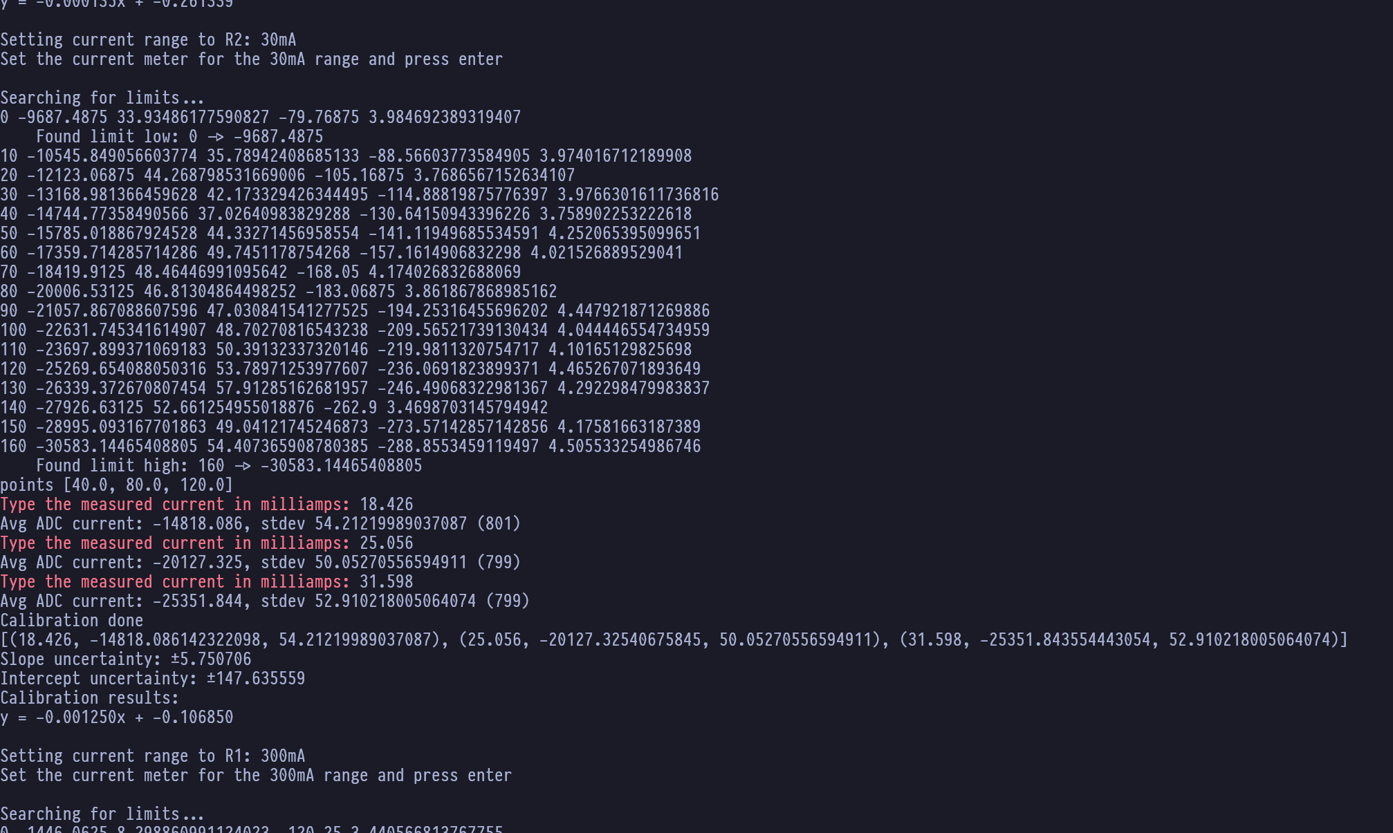
After the calibration is done the script prints the calibration coefficients in JSON format which is used by the libjellyfishopp module. It can also read the JSON calibration file and print out the calibration coefficients as .c file which is directly included into firmware.
Host app
Based on the libjellyfishopp Python module, I wrote a simple host app for data visualization (jelly_plotter.py). It's using PyQtGraph for plotting and it's showing all signals received from the device together with the real-time (filtered) voltage and current values. The app is still very simple and doesn't have options to save the data or to control the device.
Battery profiling
When developing a low power device, it's important to be able to repeatably check the functionality with battery at different charge levels by using a battery simulator. For that, the battery needs to be profiled. Profiling will measure the actual battery capacity as well as the internal resistance at different charge levels.
Batteries can be modeled in a very complex ways but the most simple one (which is also good enough for most purpuses) is to model the battery as an ideal voltage source with the series resistor (internal resistance). This internal resistance depends mainly on the state of the charge but also on chemistry, temperature and so on. With high internal resistance the battery might not be able to provide high enough current.
Battery's internal resistance can be easily calculated by measuring the voltage and discharge current at two different currents.
The jf_battery_profiler.py script can perform simple profiling of the battery. At the start it will measure the battery open circuit voltage. Then it will slowly increase the discharge current (by reducing the output voltage) in order to find the voltage levels for the defined discharge thresholds. After finding the thresholds it will switch between those two levels and calculate the internal resistance.
I performed a short profiling of three different batteries: a slightly used CR2450 coin cell, a used AAA battery and a brand new AAA battery. The results are shown in the images below.
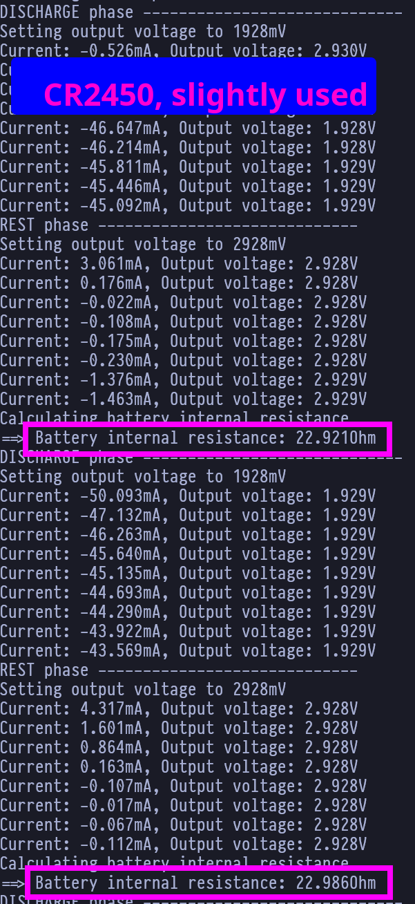
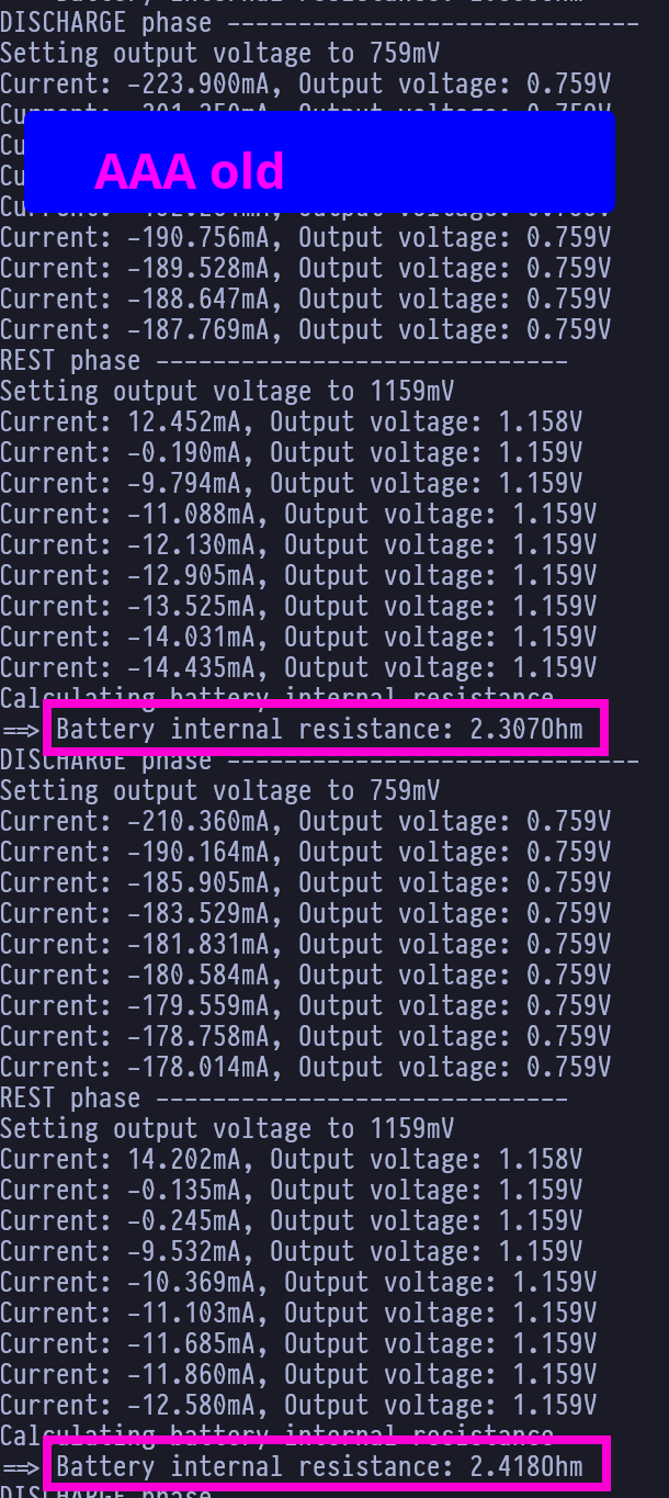
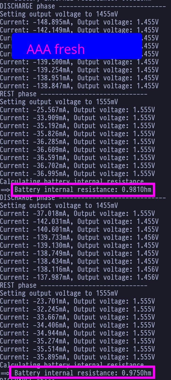
We can see that the coin cell battery has very high internal resistance. We can also see that the used AAA battery has higher internal resistance than the brand new one.
Here's the video of the profiling process:
In the future the script will be improved in a way to log the data to the file and also to calculate the battery capacity.
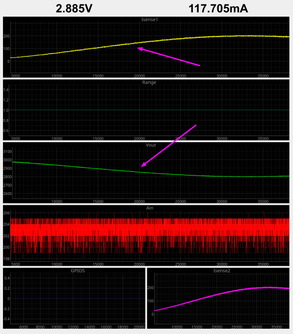
Battery simulation
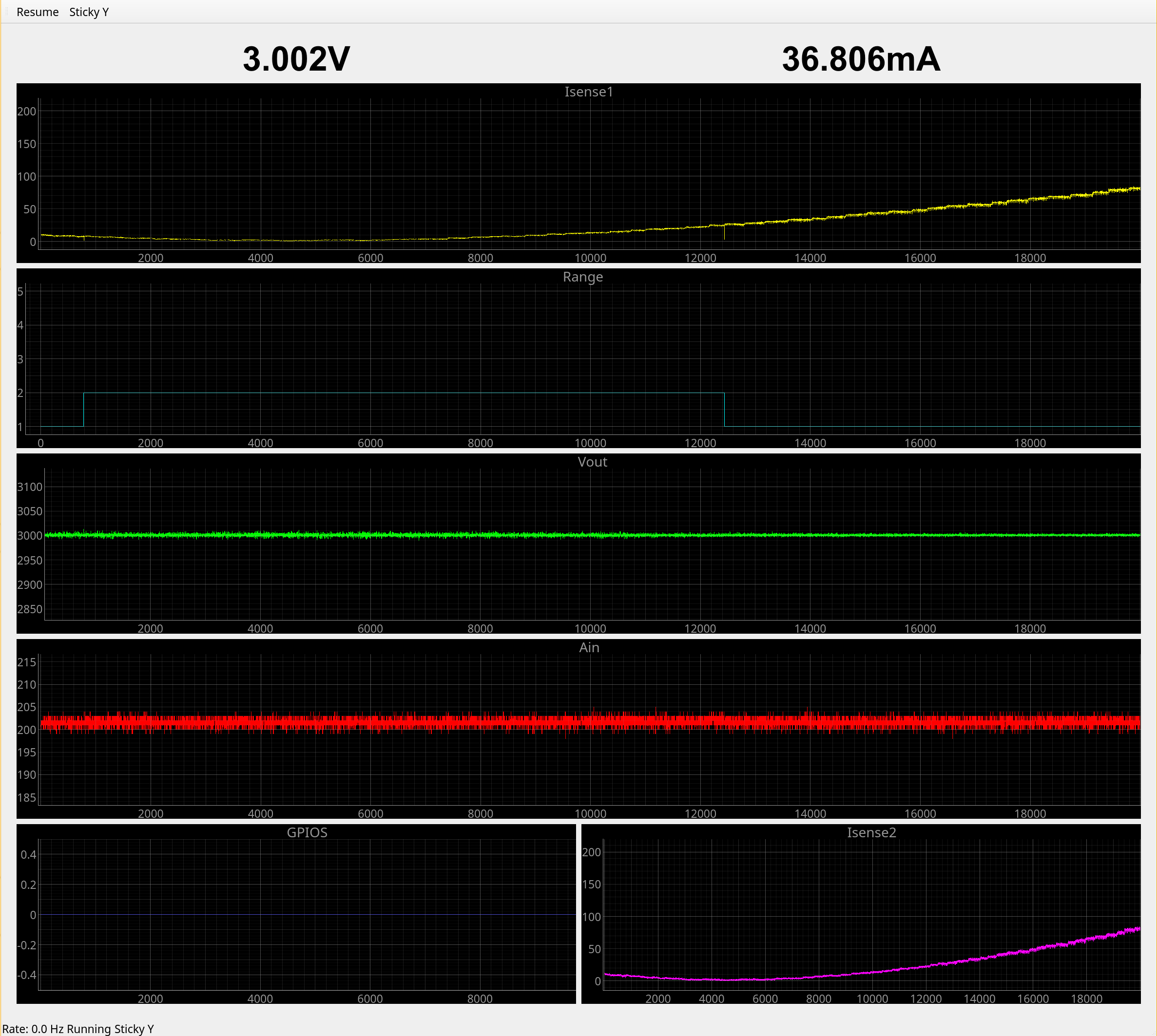
Same as the battery profiling, the battery simulation feature for now is based on the battery modelled only as an ideal voltage source with the internal resistance. In order to do this, in each sampling cycle the FPGA calculates the voltage drop on the internal resistance and then decreases the output voltage by that amount.
For this I implemented a 16-bit multiplier module for calculating the voltage drop and a moving average filter for smoothing the measured current before calculating the voltage drop (gw/src/multiplier.v, gw/src/mavg_bram.v). However, the (mostly) unexpected thing happened - I endded up using all available logic fabric of the ICE40HX1K I'm using. So, even though my code seemed to be ok there was no way for it to fit into the FPGA no matter which optimizations I tried (the first iteration of the moving average used LUTs for the buffer so I switched to using BRAM hoping that it would save enough logic cells). In the end, in order to test the feature, I had to do some cuts to the gateware: represent the internal resistance only as a power of two value (to use shifts instead of full multiplication) and disable the auto range. With that it worked!
In the image below we can see that when the current is increasing, the output voltage is dropping proportionally to the current, compared to fixed output voltage when the battery simulation is disabled. Here, the internal resistance is set to around 1Ohm (current increase of 200mA caused the voltage drop of 200mV).
Luckily, there is a ICE40HX4K wchich comes in the same footprint but it has more than enough LUTs to fit everything and which will fit the future improvements and better algorithms both for battery simulation but also for auto range switching and some other parts. I'm going to get them in my next Mouser order and replace the ones on the boards with a bigger one.
Other features
While the UI on the device is far from being complete, it still allows some basic functionality to be controlled without the need for the host machine. It can set the output voltage, set the current limit, set the AUX voltage output or enable the external input.
Currently the UI is really slow as the firmware isn't very optimized and, while the device is handling the measurements and USB data, the display has the lowest priority. That's why it has really slow refresh rate and the encode is very janky.
When the external input is enabled, the device can be used as a simple multimeter with the voltage and current values displayed on the screen. It could also be used, with host application connected, as a really low bandwidth oscilloscope.
The video of the device UI is below:
Issues
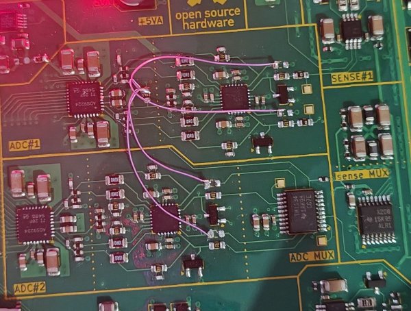
There are still some issues with the device which I need to fix. One of the minor ones is that I actually forgot to make one change for the second revision (ADC negative inputs referenced to GND instead of to 2.048V reference) but those were quite easy to rework on the PCBs (image below). Another minor one is that PCA9306 (I2C voltage level shifter) has wrong component product number specified in the design files (different footprint) so I had to manually solder them after receiving the boards.
Performance
All of the things the device is doing are taking a lot of resources and the STM32F446 MCU is struggling to handle it all. Currently the biggest resource hogs are periodic interrupt which is getting the data off of the FPGA and a USB data transfer from the device to the host. USB transfer is using a max buffer size of 512 bytes so there's not much to do there. But the data transfer from FPGA is storing the buffer into block RAM which is 4096bits (256 bytes) in size. There is a much bigger SRAM chip on the device so the next step is to use it for storing the data buffer. That way the number of timer interrupts will be greatly reduced (the actual transfer is using DMA) freeing the resources for UI and other tasks.
DC/DC
The new prototypes came with a strange issue with the DC/DC converters used for converting the system voltage to the 5.5V and 3.3V. For some reason, when the system voltage is higher than 12V it starts heating up quickly and it overheats at around 15-16V. The DC/DC converters are based on TPS54202 buck converter from Texas Instruments. Since those parts haven't changed since the first revision at first I thought that the fab house used fake chips. Another fact supporting that idea was that, after I replaced one chip with a new one I ordered from Mouser it stopped overheating and is working normally through the whole input voltage range (up to 20V). But after I also changed some other chips with the new ones, some are still overheating. I don't currently know the real reason and don't have any more spare chips to replace so I'll do further tests after I order some more - I haven't really took notes on which chips I replaced, as I was also doing some other things at the time, so it might still be the fake chip issue but I'll do more checks.
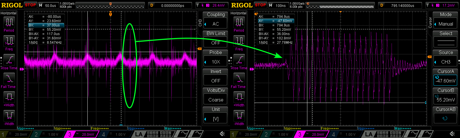
Noise
The noise (both at the voltage and current readings) is higher than expected. Also, on the main output there is some noise periodically happening (with some short bursts). It's definitely coming from some digital part but I haven't yet figured out exactly what is causing it. The plan is to check the output voltage while disabling some parts of the device and also to check all other clocks and data lines to find what correlates with this noise. The fix will probably include some additional filtering.
Sampling rate
Current sampling rate of the main ADCs is around 75kHz. There are few reasons for that but it is relatively easy to increase it 2-3 times.
The ADCs support a couple of ways to get the data, from the basic SPI to enhanced SPI (with up to 4 data lines) and parallel transfer with 8 data lines (all of the data lines are connected to FPGA so all of those methods are supported). All methods other than basic SPI require some initialization over SPI which I was lazy to do when I was writing the ADC control Verilog code for the FPGA. I started with the idea to use the basic SPI and increase the FPGA clock speed from 24MHz input clock to 96MHz using the PLL as that would get the sample rate over 300kHz after which I would rewrite the code to use one of the more complex methods to increase it even further (ideally to 1.5-2MHz). But after spending a lot of time trying to configure the PLL without success, I found out that even though FPGAs are very flexible with the pin mapping, there are still some rules regarding the clock. Basically the PLL peripheral is clashing with the IOB_35 pin which is used for the QSPI clock. The only option to increase the FPGA clock speed is to actually give it a faster clock - it's currently using 24MHz oscillator which is shared with the USB PHY so even though I can easily increase it (it's generated by MCU), the USB PHY requires 24MHz so I would need to separate them to different clocks).
For now there's no need to increase the main clock as the first step is to rewrite the Verilog code to use the faster transfer method (actually, due to the way I wrote the current Verilog code, the real ADC clock is 12MHz, so even the basic SPI when properly implemented to use the full clock speed would double the sampling rate). The only reason I haven't done that part yet is that I can still do everything I need for the development even with this so it has a bit lower priority.
Measurements
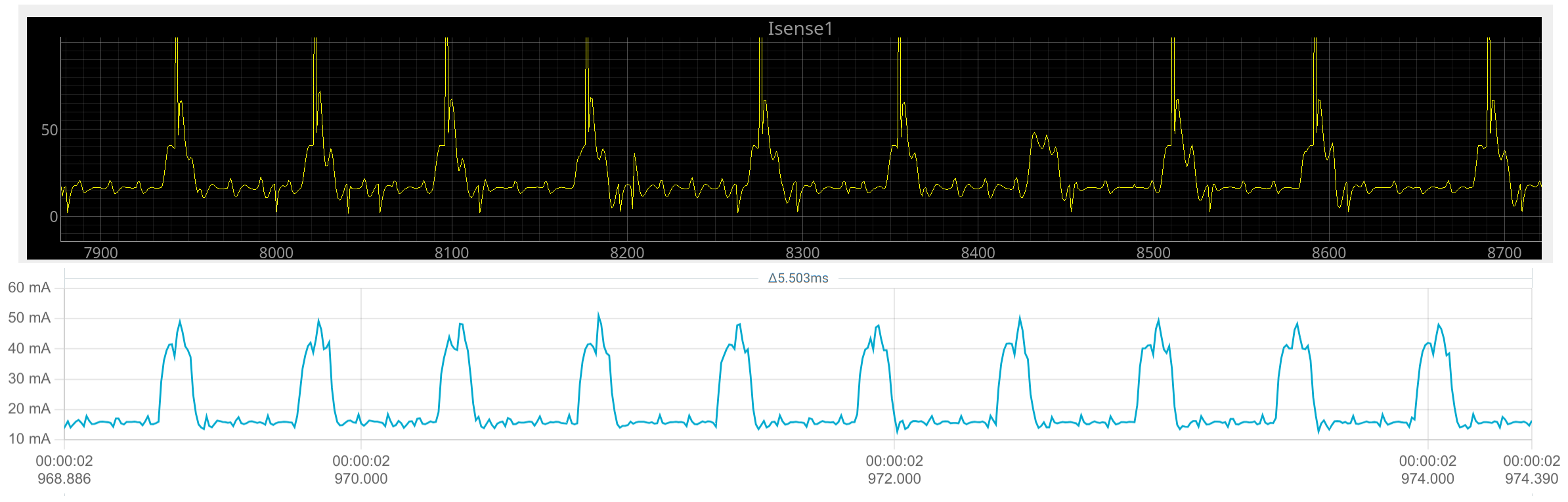
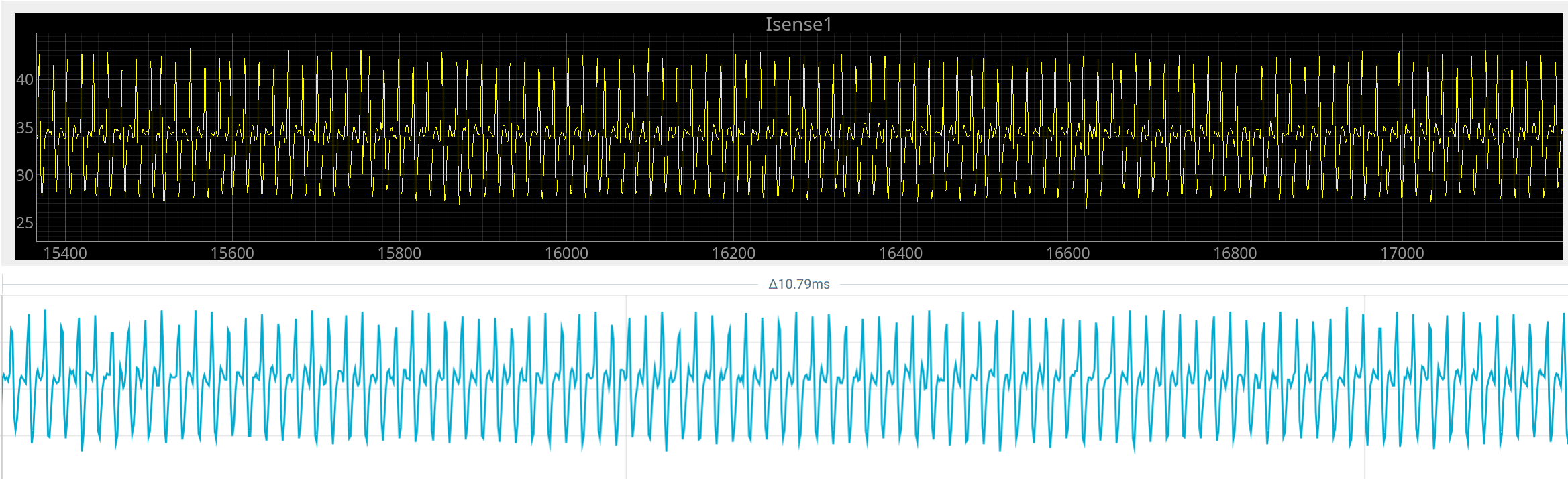
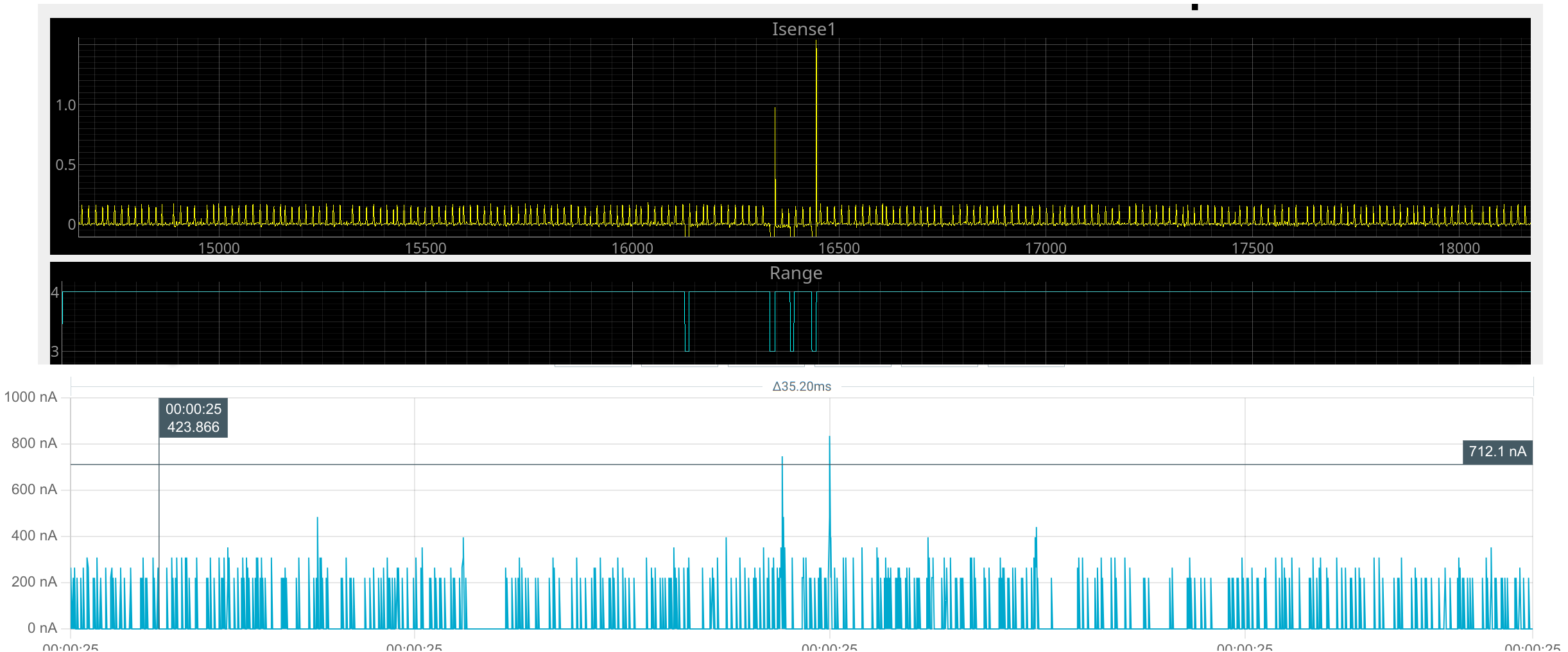
I did a small comparison of the measurements between the JellyfishOPP and Nordic PPK2 - JellyfishOPP is providing the power and has PPK2 connected as ampere meter in series with a test board. It was a bit tricky to sync them to show the same timespan as the Jellyfish app still doesn't have a lot of required functionalities (for example longer history view). The results are pretty good connsidering that JellyfishOPP still needs some work both for range switching and for measurement noise improvement.
The first image shows the Soldered Dasduino board PWMing a LED. While not identical the peaks look very similar. Jellyfish trace has additional spike caused by the range switch which will be fixed by improving the range switching algorithm.
The second image shows a small Lora sensor board while doing the transmission. Here there's no range switching and no spurious spikes. The PPK2 trace has y-axis labels cropped out but they show the same values.
The third image is the same Lora board during the sleep mode and both devices show the same two peaks. Here I included the range switch data too. The displayed magnitudes are a bit different but that will be improved after fixing the noise issues.
These are just the preliminary tests and I'll do more tests after fixing the higher priority issues.
Summary
That's all for this update. As usual, all of my time estimations up to now were very wrong so I won't give any estimates for the next update. But I'll keep working on fixing the above mentioned things.
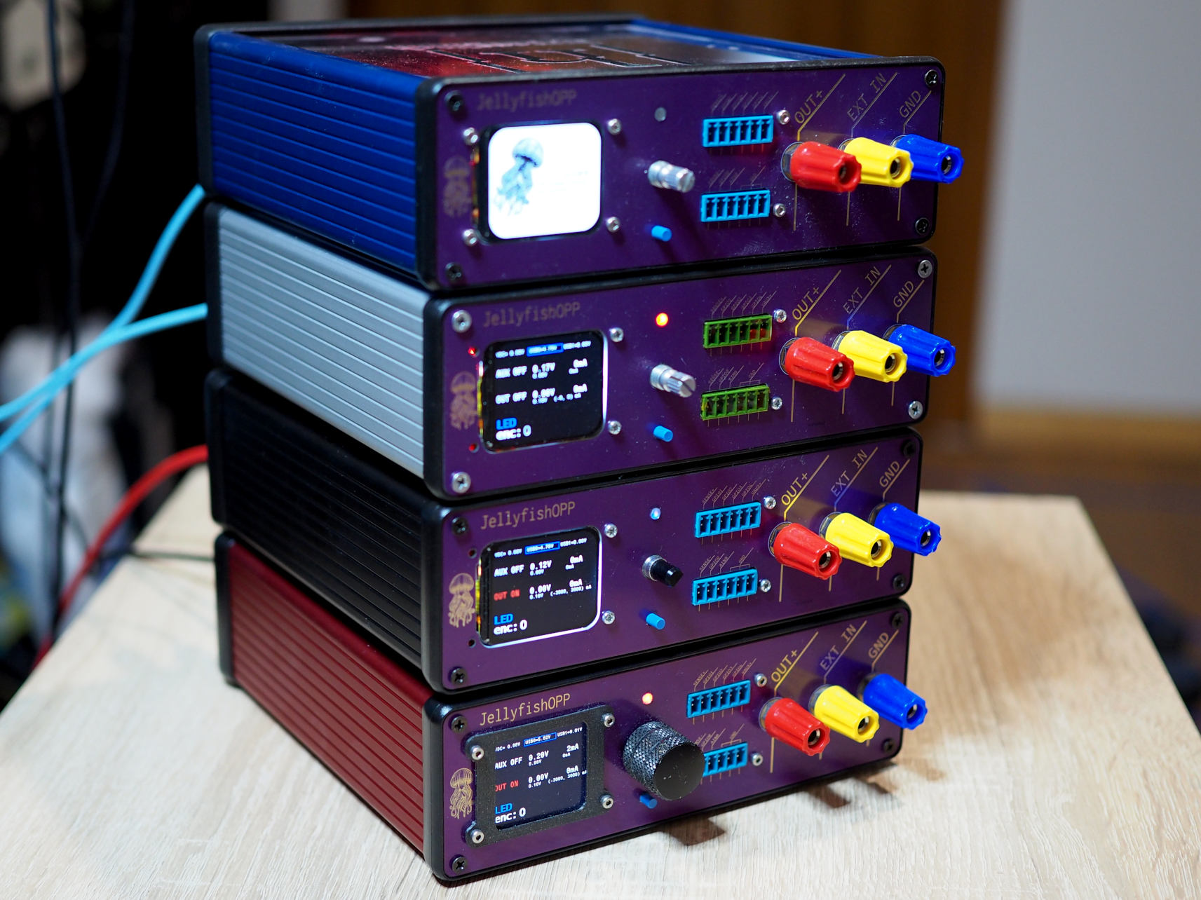
Also, since now I have three devices, the hardware pretty much works (with some minor issues) and the firmware is already usable, I'm planning on making some official communication channel for real-time communication (probably on RADIONA's Discord) and this is also the phase where I want to start looking for some contributors.
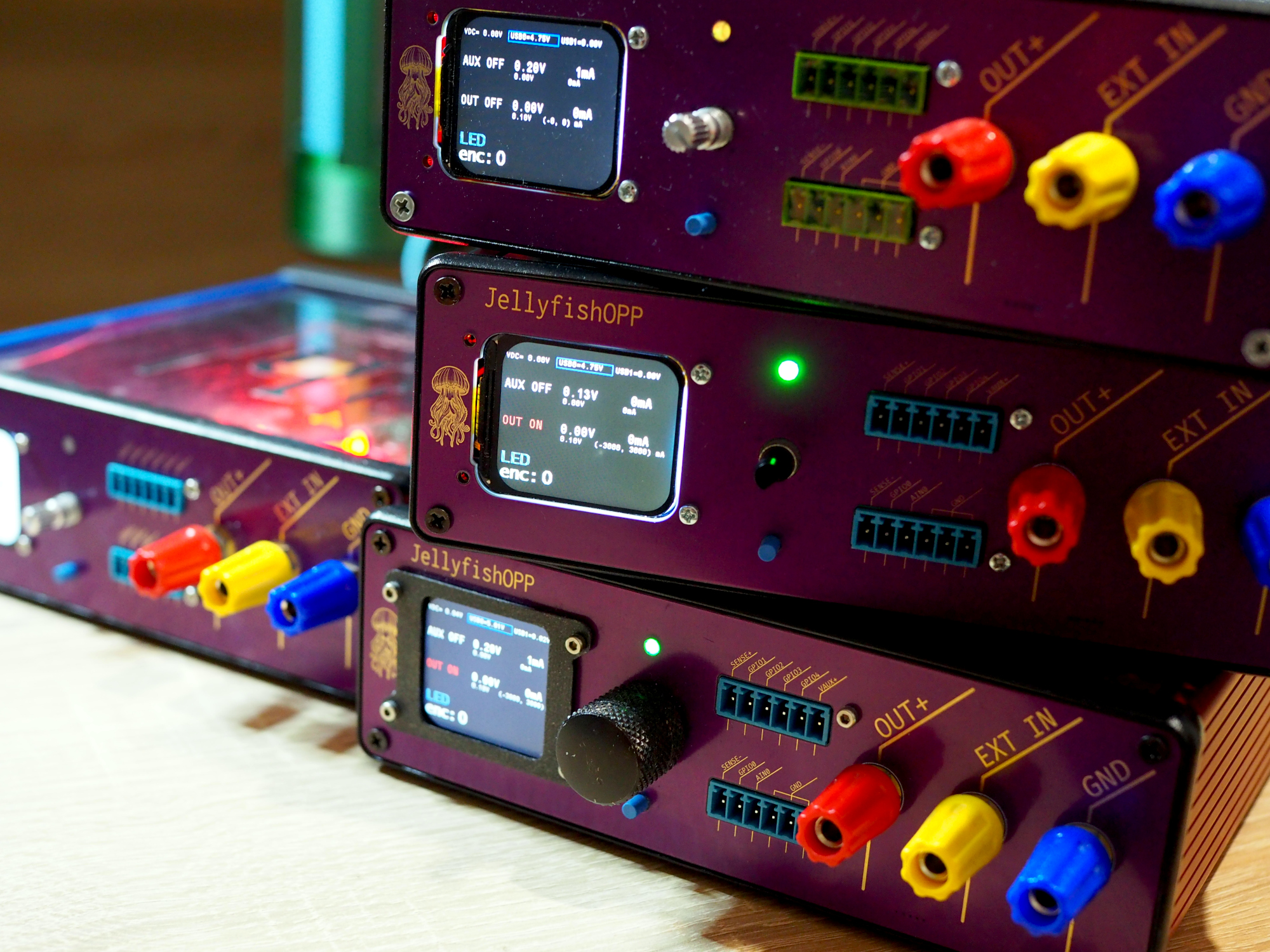
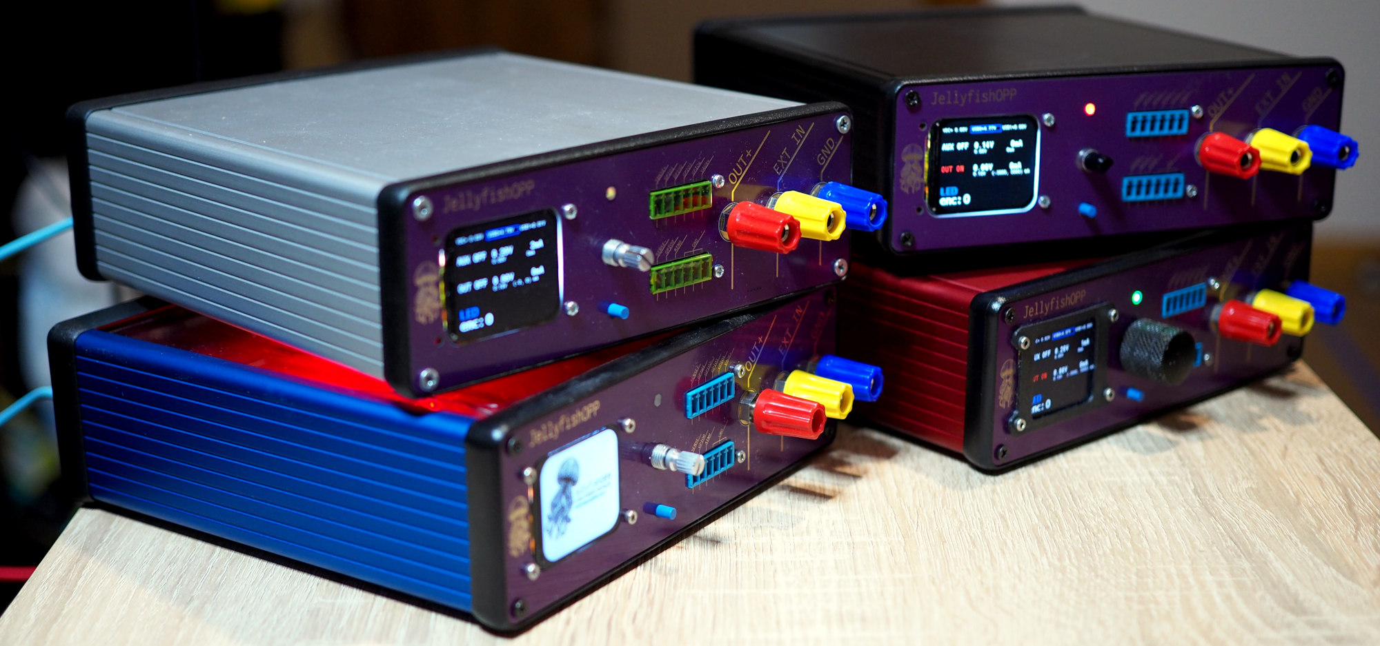
For the end, here are two more pictures from the JellyfishOPP photoshoot (I had some issues with my 3D printer so I couldn't print the screen bezels :)).