Intro
This took a lot of time... I made a lot of progress and also found a some mistakes in the design. Here's a summary of the rest of the testing with the focus on fixing all hardware mistakes on the prototype. This part was done mostly in parallel with the FPGA part but I've split it into two articles to have them thematically separate.
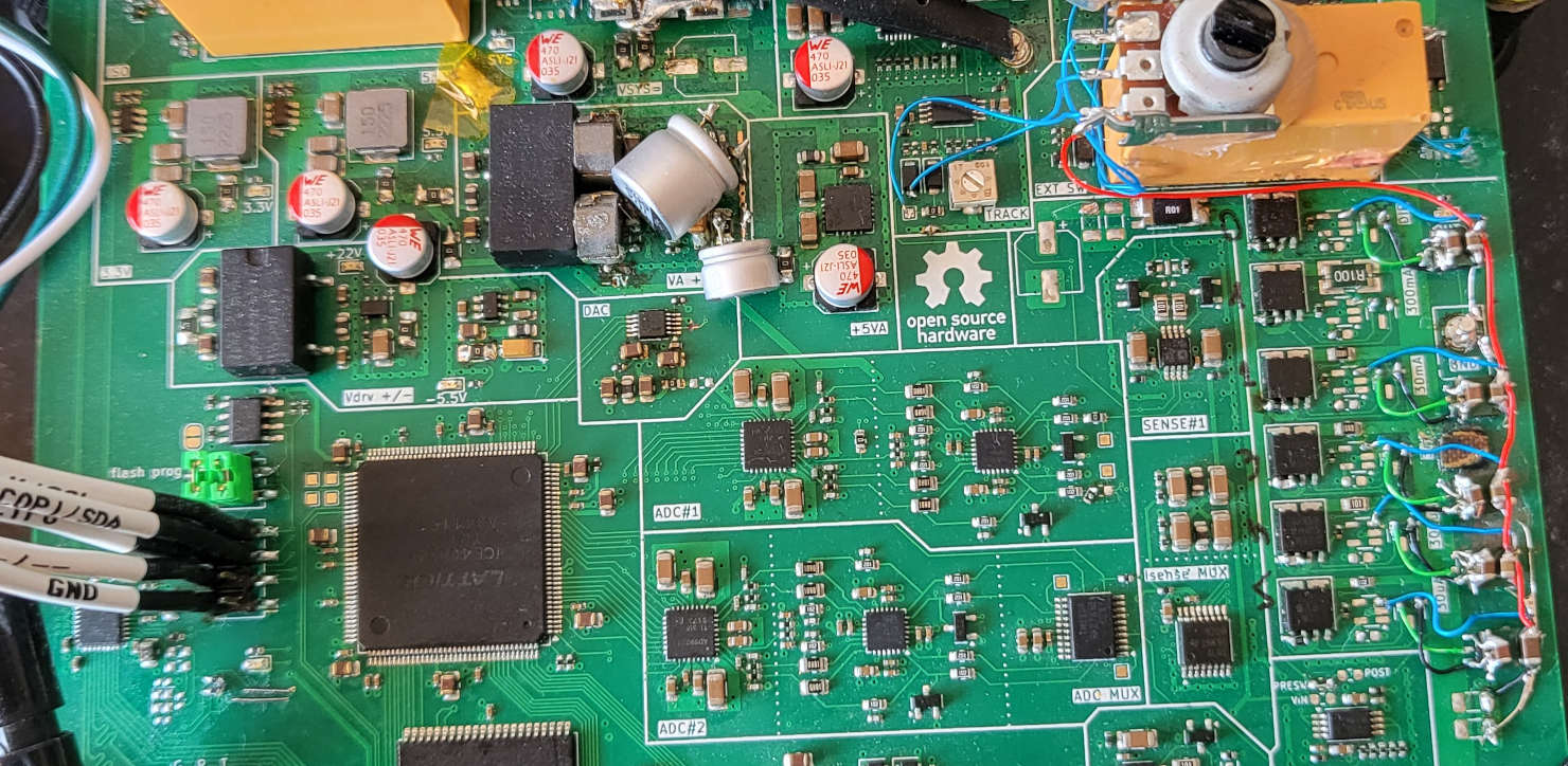
Shunt/range switching
For the range switching there are five parallel lines with different shunt resistors and one direct line without the resistor. The shunt resistors are switched in line with two back-to-back MOSFETs. Since the MOSFETs are in line with the output, a high side gate driving is needed to turn them on or off.
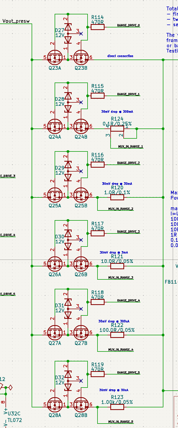
The original MOSFET drivers for range switching were a complete failure. Now looking at it, I'm not even sure why I thought that they could work at all. I mean, they did work but they were injecting a lot of current into the output. In theory (and in the simulation) it worked but in practice with the high Vgs and limiting Zeners it was a complete disaster.
I had few options in mind here: to try using the high side driver with a charge pump (MIC5012YM), to try to use a standard high side driver but with a floating supply in place of the bootstrap capacitor or to try make a fully floating gate driver. The issue I had with the first and second approach was some current leaking into the output (in addition to the undervoltage protection level on most gate drivers which is set to at least 9V). The MOSFETs used for range switching are logic level MOSFETs so just a few volts is enough to turn them on. So it was up to the third approach.
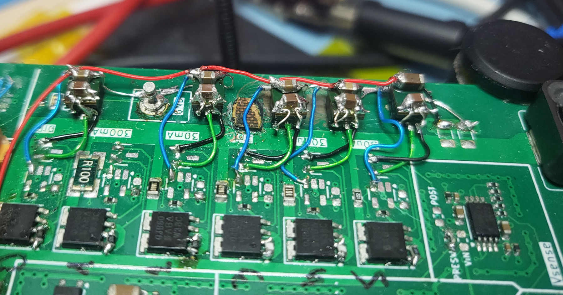
Initially I wasn't looking forward to the fully isolated floating gate drivers due to the number of required isolated DC/DC converters (and their size). But then I found two pin compatible super small 5V isolated DC/DC converter (MPS MIE1W0505BGLVH, and RECOM R05C1TF05S-CT, 5x4mm, 1W). They have a really bad efficiency but I don't need to draw any significant current from them so it should be fine for this). Testing this idea by using a small LiPo battery connected directly to the MOSFET gate gave promising results. In addition to the DC/DC converter I added a high speed optocoupler with push-pull output (Toshiba TLP2345) to act as an isolated gate control. This optocoupler can sink and source up to 50mA which is good enough to switch these MOSFETs directly, without the need for additional transistor.
Testing this approach required to some board rework. The DC/DC converters are just a bit smaller than the SO6 package of the optocoupler so I did some stacked dead bug rework directly on the board with the optocoupler at the bottom, DC/DC converter on top of it and input and output capacitors at the top (there's a leftover from a first test of the DC/DC converter glued to the board which I wasn't able to remove).
Compensation
While testing the current limiting capabilities I noticed the oscillation on the MOSFET gates of the main output stage when the current limit was reached and the output is shorted to GND. The same behavior was also happening when I connected the electronic load to the output (i.e. any low impedance sink). After some investigation it turned out that the voltage control and the current control regulators are fighting each other and causing the oscillations.
The U23B is a buffer for the voltage control signal and the transistor circuit on the right hand side is the voltage control loop, trying to keep the output at the value set by the Vset signal. The U22A and U22B are taking the Isense (amplified current sense signal from the first 10mOhm shunt) and comparing it to the positive and negative set points. If the Isense is greater than Iset+ or lower than inverted Iset- the U23A output modifies the Vset until the current is inside the set limits.
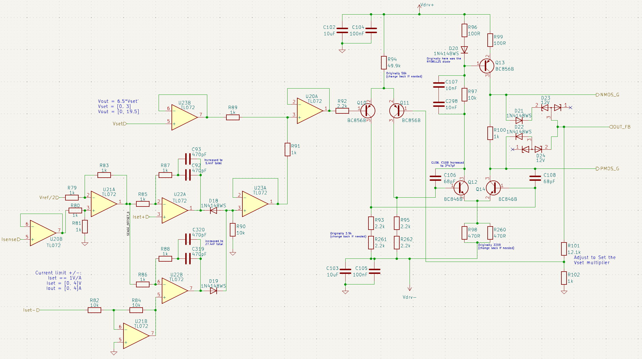
Long story short, I needed to slightly slow down the current limiting feedback by increasing the value of the capacitors on the U22A and U22B feedback lines. This reduced the output bandwidth and will need to be further adjusted but for now it's good enough. Also, the mistake I did was to wire the device output (after the sense resistors) as the voltage feedback line for the regulation. I did this in order to minimize the burden voltage of the current measurement (i.e. to compensate for the voltage drop on the shunt resistors) but this doesn't work when the output is shorted to GND. This was also the cause of the oscillations and connecting the voltage feedback to the Voutpresw helped a lot (this in fact increases the burden voltage which I was trying to compensate by taking the feedback from the output but since it's limited to 30mV for each range it should be fine).
I might reconsider using the power opamp instead of the transistor based output control circuit in one of the future versions of the design. I liked the transistor based design as it solves the crossover distortion and enables setting the output voltage below 0.6V (which provided the smooth output value around 0V for the 4-quadrant version where the output could go to negative voltage). Using the power opamp would increase the output bandwidth and simplify the design but would set the minimum output voltage to around 0.6V (which could probably be ok).
Leaking output
The good thing about developing the low current measurement device is that it can be used to troubleshoot itself during the development. I noticed that there is a current flowing through the sense resistors (i.e. the current sense amplifier was giving a significant value at the output) when the output isn't connected to anything. It wasn't a lot of current (around 60uA after the MOSFET drivers were removed) but if the goal is to measure sub-microamp currents then it is a big deal. Also the output current wasn't constant, it was slowly decreasing. That made me realize that there is some capacitance on the output being charged.
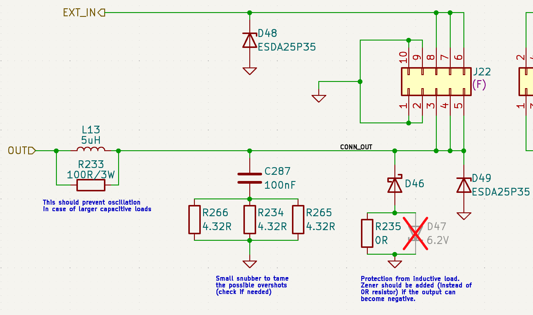
I started this by setting the measurement range to one of two lowest ranges and measuring the current sense output. The culprit for the slowly decreasing current was the output snubber. The source of additional leaking were the Schottky diode used for protection from inductive loads and the TVS protection diode. After removing them the output leakage dropped to under 300nA which still isn't perfect but it's acceptable. I found that Texas Instruments TVS2200 is a super low leakage (3.5nA @ 25°C) 22V protection diode. I should still find some low leakage power diode for the protection from the inductive loads.
Conclusion
With these modifications in place now the complete hardware of the JellyfishOPP is tested and working. The next step is to implement all of the design changes into the schematic/PCB and order the next revision of the board.