Intro
In the last article I mentioned that I basically had to write most of the FPGA code just in order to verify the peripherals (range switching, ADCs, DAC, etc.).
Before writing the communication code, I needed a way to signalize something from the FPGA. Since I can't just attach the debugger to it and stop the execution I needed some other way to send back some info, without relying on QSPI since that wasn't done yet (and I need a debug method which I can use for that). I could simply toggle some pin but I wanted something easier to read without attaching the scope so my first real FPGA module was number_blinker - a module which blinks a LED some number of times, makes a short pause and repeats the process. This made it easy to send different number of blinks from the various places in the code.
FPGA - communication
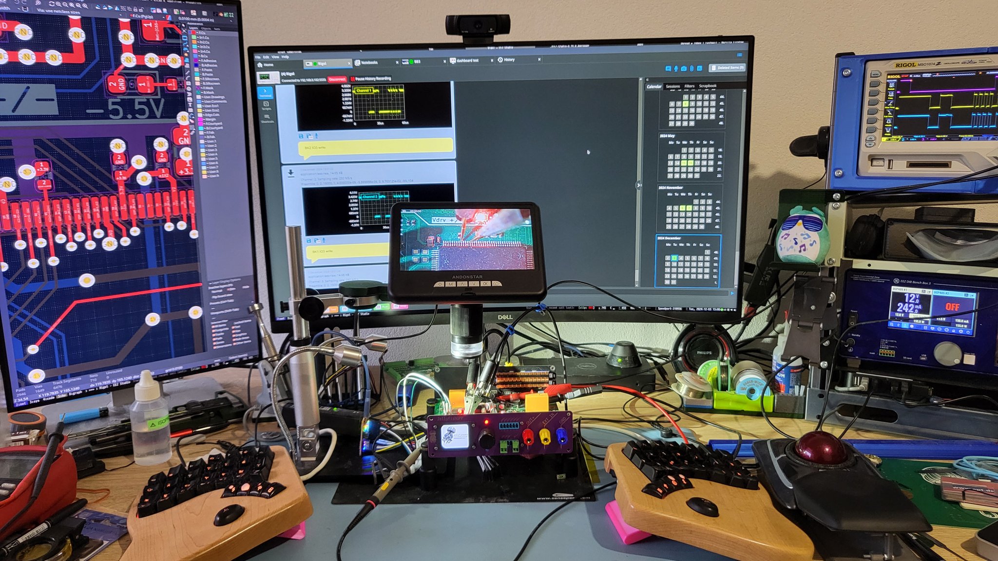
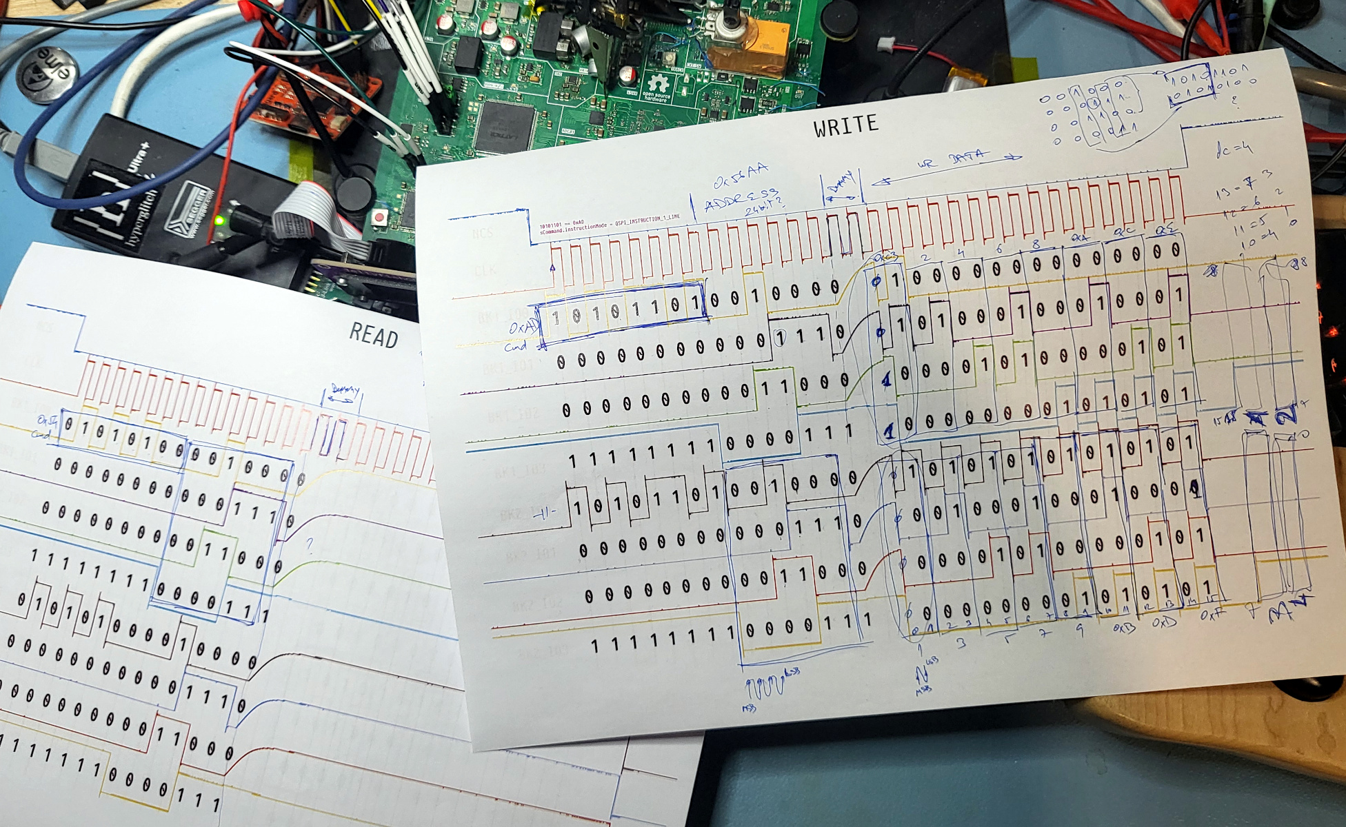
So, after the "better blinky" was done, the next thing was to write the communication code between the MCU and the FPGA. The comunication is done over (dual bank) QSPI. In order to do that I first had to record the actual communication to figure out what's going on on the wires and then emulate that from the FPGA. Since the data lines are bidirectional I wanted to use oscilloscope to properly record the lines switching to Hi-Z mode. And, since the dual-bank QSPI has 10 wires in total (and I have four inputs on my oscilloscope but also it's quite hard to fit more than three probes on the chip pins) I did it in multiple takes, recording two-by-two lines both for read command and for write command, using NCS line as a synchronization. For data recording, as always, I used the Envox EEZ Studio. From there I exported the data as CSV, did some post-processing and plotting in Octave and finaly slightly edited the images in Inkscape and printed them out on paper so I could easily annotate it. For the address and data payload I used some bit patterns which I could more or less easily recognize in both directions which was important when figuring out how the bits are set on the wires.
After figuring out the QSPI it was time to implement it in the FPGA. I knew a few things about clock domain crossing in the FPGAs but I never ran into it. But here we have FPGA's main clock which clocks everything and the communication is done on the QSPI clock. Hard thing about clock domain crossing is that it's not that easily detectable (Goran told me about CDC snitch but I haven't tried it yet). So, after I wrote the whole QSPI state machine which worked perfectly in the simulator (iverilog), after I uploaded it to the board it wasn't showing any signs of life. That's when I realized I had a CDC problem. Luckily, it was easily solveable by just passing the signals through a two-step synchronizer (two flip-flops in series clocked by the destination clock). But it took some time to solve.
The video below shows the number selection on the screen using the encoder, sending the number to the FPGA and the FPGA decoding the communication and blinking the LED using a number_blinker module. It's not much but this was a significant milestone in which I solved the hard issues with FPGA and after that it was (mostly) smooth sailing.
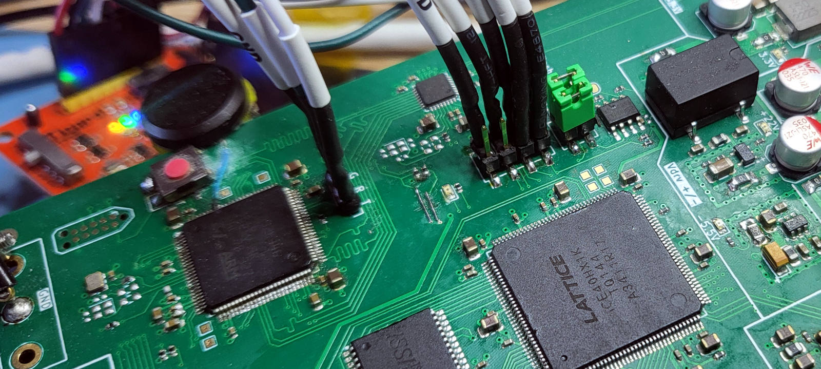
Another one of the challenging issues was changing the direction of the pins mid-communication when sending the data back to the MCU. First try was to just set the data pins as inout and then either set them to Hi-Z for reading or set them to some value for writing from FPGA. This again turned out to work in the simulator but not on the actual board. I realized I can't just use the pins directly for this purpose and that I need to use ICE40 specific primitive called SB_IO which is a three-state buffer attached to a pin. After some more messing with the code I managed to make it work. This, off course, made the testing more complicated as, since the SB_IO is ICE40 primitive and not available in standard Verilog, I had to implement it in the test code.
The rest of the FPGA modules
After solving the main challenges, namely communication, clock domain crossing and three-state buffers, it was time to implement the rest of the required modules for testing. They were mostly straightforward (compared to initial ones).
At the center of the whole architecture there is a demux8 module - a simple demuxer which, after receiving the command over QSPI, will send a trigger signal to one of the other modules based on the specified command (for example, command 0x05 will send the payload to number_blinker, command 0x04 will control the range switch, command 0x06 is controlling the DAC and so on).
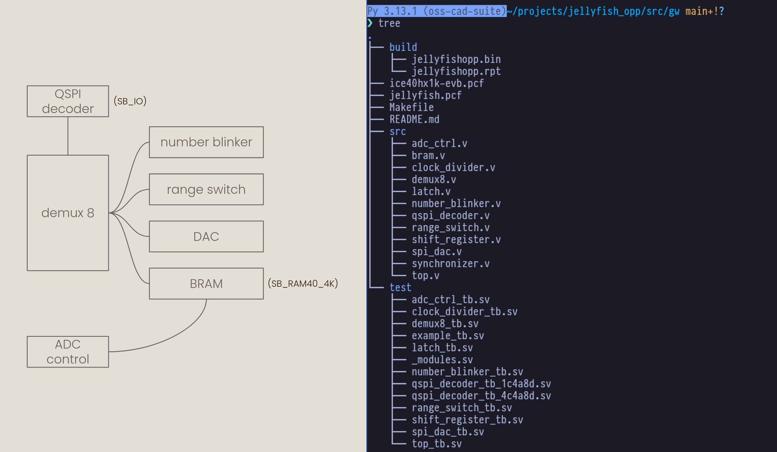
range_switch module is responsible both for enabling the correct shunt resistor as well as set the multiplexer to bring the correct measurement line to the ADC input. dac is a simple SPI DAC used to control the output voltage regulator. adc_ctrl controls the ADC by initially setting the configuration registers over single line SPI and then fetching the data in parallel over multiple data lines. The conversion result is stored into the buffer created in the block ram (SB_RAM40_4K ICE40 primitive) so it can be read back by the MCU. Although the functionality is confirmed the dac and adc_ctrl modules still need ironing out some of the details.
Conclusion
The FPGA part was quite challenging and I had to spend a lot of time on it but in the end it was a success. Most of the stuff I learned from the Getting started with FPGAs book by Russel Merick and it gave me a good initial overview of the process. Also ChatGTP helped a lot with the technical details of the implementation.
On February 19th RADIONA held an FPGA meetup in Zagreb where I presented my experience with FPGA development for the JellyfishOPP from the point of view of a FPGA beginner. The video of the talk is available below.