I realized that it's been quite a while since I last posted about the project's progress. A lot has happened in the meantime, so here's a brief overview.
Although not directly related to the progress, I had the opportunity to present the state of the JellyfishOPP project at the Balkan Computer Congress in Novi Sad, Serbia from September 20-22, 2024. The video of the talk was recently published and it's available here: https://www.youtube.com/watch?v=dX2E_3WZqq0
Prototype
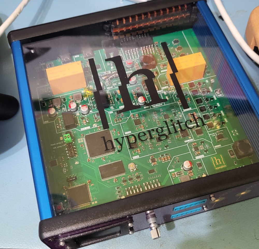
I received the assembled PCB of the first prototype in August.
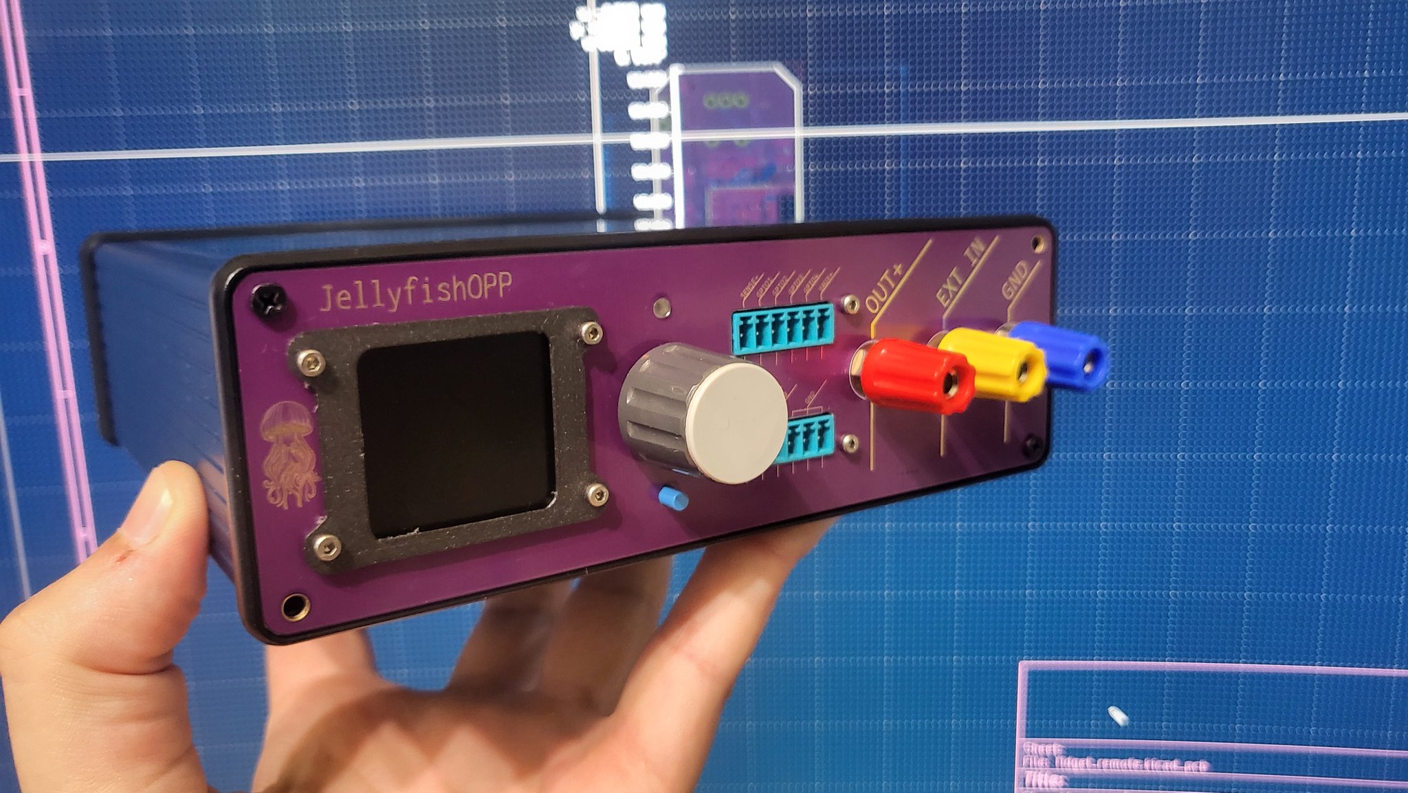
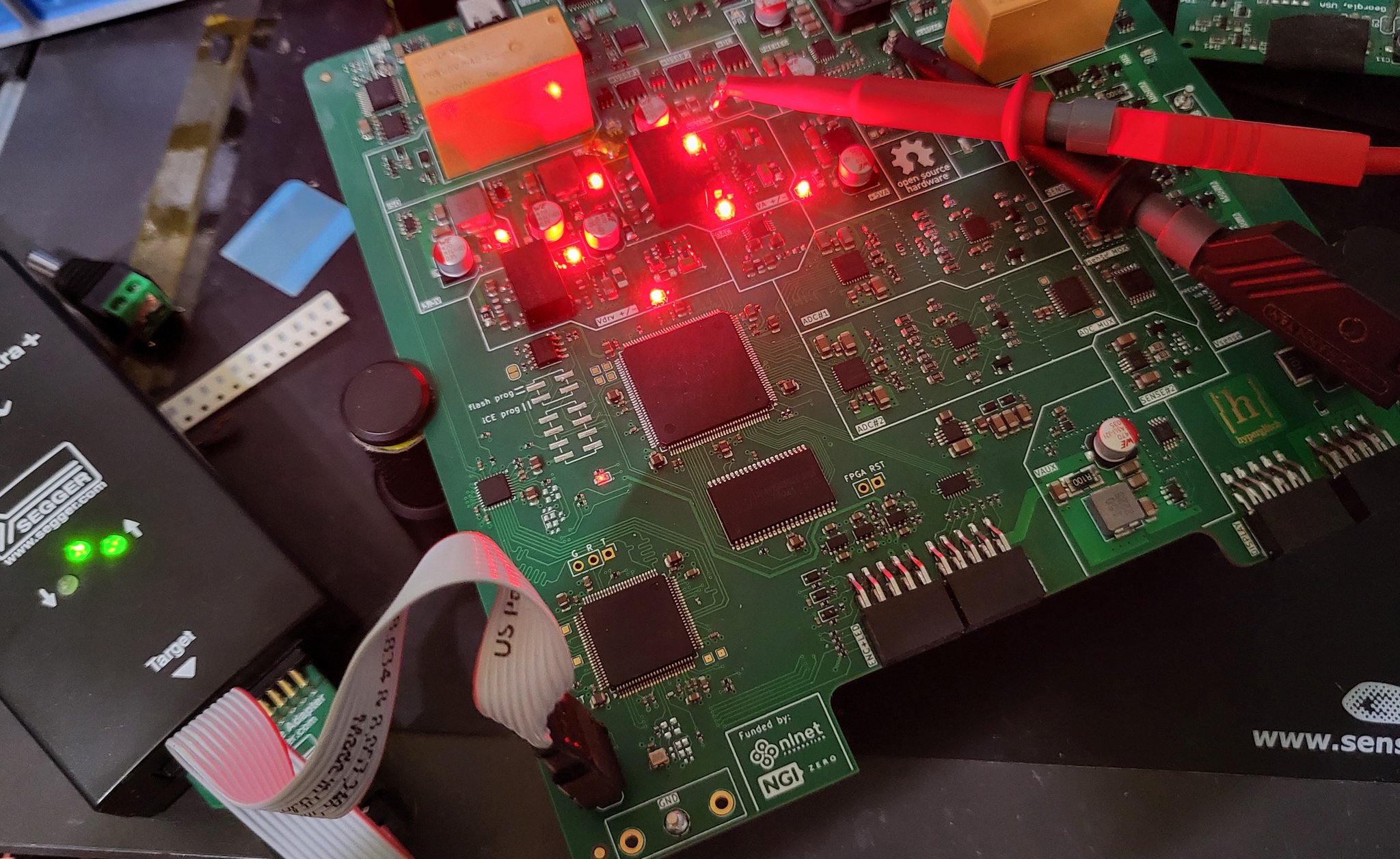
The good news is that there were no major or obvious issues with the PCB. All of the power supplies had 0Ω resistors on the input and output, which made it easy to verify each one separately before powering the whole board. All the power supplies worked, except for the high-pitched squealing of the +/-8V regulator (more on that below).
The MCU was also functional. I was able to program it and verify basic functions like LEDs, the encoder, push buttons, serial communication, and the display. I then proceeded to test the AUX power supply (including voltage and current measurement), the power pre-regulator, maximum current loads on the power supplies, and FPGA programming (both the internal SRAM and external flash).
I also experimented with running the Zephyr OS on the MCU and successfully tested some peripherals with it. However, since I'm not yet very familiar with Zephyr OS, and since this is a custom board, I had to spend quite some time writing device tree definitions. This was time-consuming, so I switched back to ST's HAL library and FreeRTOS for the rest of the verification. I may revisit Zephyr OS once the functionality is fully verified.
Hardware mistakes
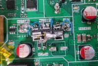
There were few mistakes in the hardware design that I had to address. The first one was with the input power selector. It turned out that I put the MOSFETs (which were suppose to act as ideal diodes) in the wrong orientations (which made them behave as regular diodes). A bit of rework (first image below) fixed that. "Fun" thing: after fixing the power ORing part, I went to double check everything. It was already past 2AM (and nothing good ever happens after 2AM) and I was checking some pins with multimeter probe and accidentaly shorted the 15V from the input to one of the VSENSE pins going directly to the MCU which, of course, fried the whole MCU. And replacing the 100-pin LQFP package is really not fun, especially since the fab house used some higher temperature solder paste and this is a 6 layer board with a lot of copper inside. Lesson learned: always add inline resistors to MCU pins.
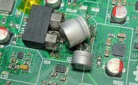
The second mistake is related to the +/-8V regulator. The high pitched squealing was really annoying. After some poking around I realized that the output ripple was way too high. My first thought was that it was due to the isolated DC/DC converter (those converters aren't the most efficient) but after some more debugging I realized that I only put the tantalum capacitors (with some 6Ω of ESR) at the output of the linear regulators while they required low ESR (<0.1Ω) ceramic capacitors. Adding the 10µF ceramic capacitors and additional 470µF electrolytic capacitors on each rail fixed the issue of the high pitched squealing and the output ripple. I also improved the CLC pi-filter between the DC/DC regulator and linear regulators by increasing the inductor value (second image).
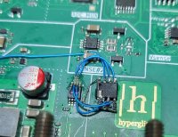
Third mistake was on the AUX power supply and it was quite stupid mistake - the I2C lines are pulled up to 3.3V and the digital potentiometer is powered from 5.5V. With the 5.5V supply, the required high level threshold was above 3.3V. The fix was to add a voltage level translator on the I2C lines (third image).
The rest of the system
Since the most of the power output/measurement sections are controlled by the FPGA, I have to write pretty much all of the FPGA code in order to verify those sections. That turned out to take a lot of time and I'm still on that (the fact that I haven't worked that much with Verilog in the past also isn't helping :)). The thing I'm working on right now is the QSPI communication between the MCU and the FPGA which will allow me to send commands to FPGA peripherals and receive data from them. QSPI is also a bit tricky since the lines are bidirectional and, since I didn't add inline resistors to data lines (to say it again: always add inline resistors to MCU pins), wrong sequence could cause short circuit. But, since I'm using dual bank QSPI (with 8 data lines) I can make it sort-of directional with 4 lines in one direction and 4 in other and then add the inline resistors in the next revision of the board. After I'm done with that I'll be able to use it to control the output DAC, the range switching and the ADCs. After that part is verified/fixed/measured I can start working on a proper firmware.
