This article will present the PCB design of the first prototype of the JellyfishOPP device. The design presented here is ordered as first prototype for testing.
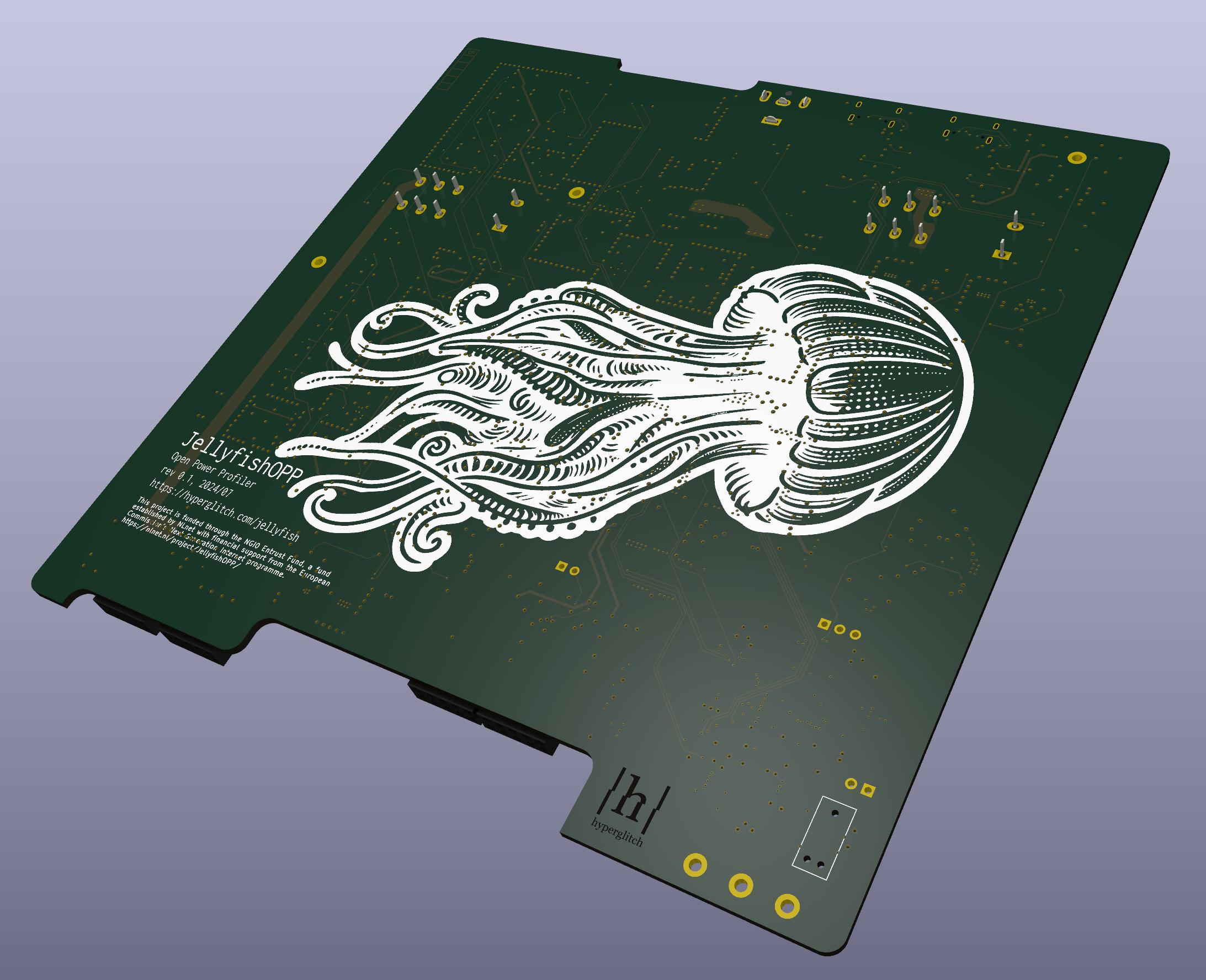
JellyfishOPP is an open source, open hardware, programmable power supply and measurement device. The main page containing the description and links to all of the development updates can be found here: https://hyperglitch.com/jellyfish.
Development of the device is funded by NLnet through the NGI0 Entrust fund. Learn more at the NLnet project page.
Table of Contents
Overview
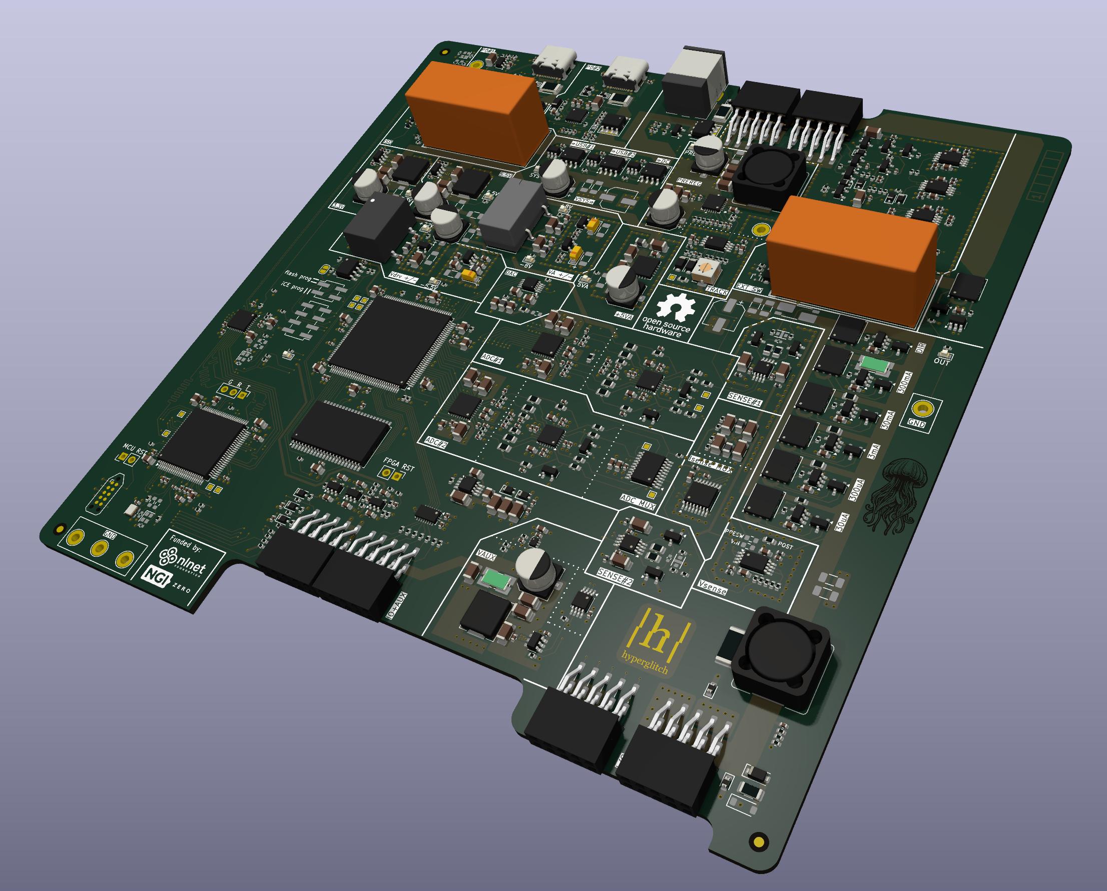
Although there are many components on the board and there are many sections, most of it is the standard stuff. There are few higher speed signal groups on the board:
- USB2.0-HS signal (90Ω differential impedance to support high speed of 480MBit/s)
- ULPI connection to MCU: 60MHz signals, trace length matched to +/-1mm and routed as (approximately) 50Ω tracks. The propagation speed is 50-70ps/cm and the recommendation for ULPI traces is to keep them all within 50ps (basically, allows for 10mm length difference).
- QSPI connection between the MCU and FPGA
- parallel interface between the FPGA and RAM (haven't length matched these but they are much slower than ULPI)
- enhanced SPI between the FPGA and ADCs
There are also some sensitive analog signals on the board (current sensing, amplifiers) which I tried to move as far as possible from the noisy and fast switching parts and leave a lot of space between traces to minimize the crosstalk and induced noise.
Stackup
I went with 6-layer stackup (top/GND/signal/GND/power+GND/bottom) for the PCB:
- top copper layer - most of the routing: power supplies, analog circuitry, ...
- GND plane
- signal plane - communication traces, control siggnals
- GND plane
- power plane + GND fills
- bottom copper layer - mostly some "slow" signals crossing the whole board
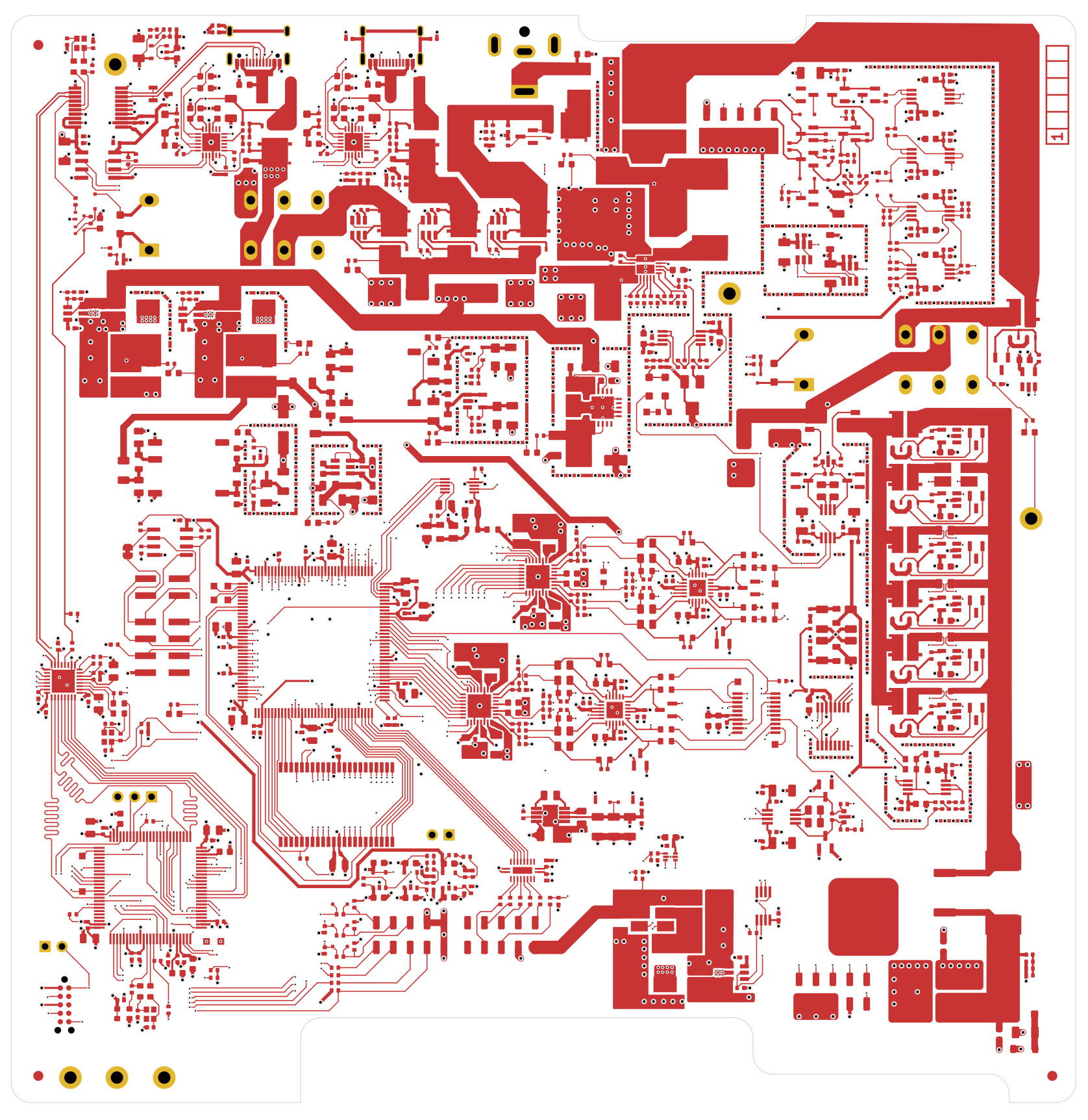
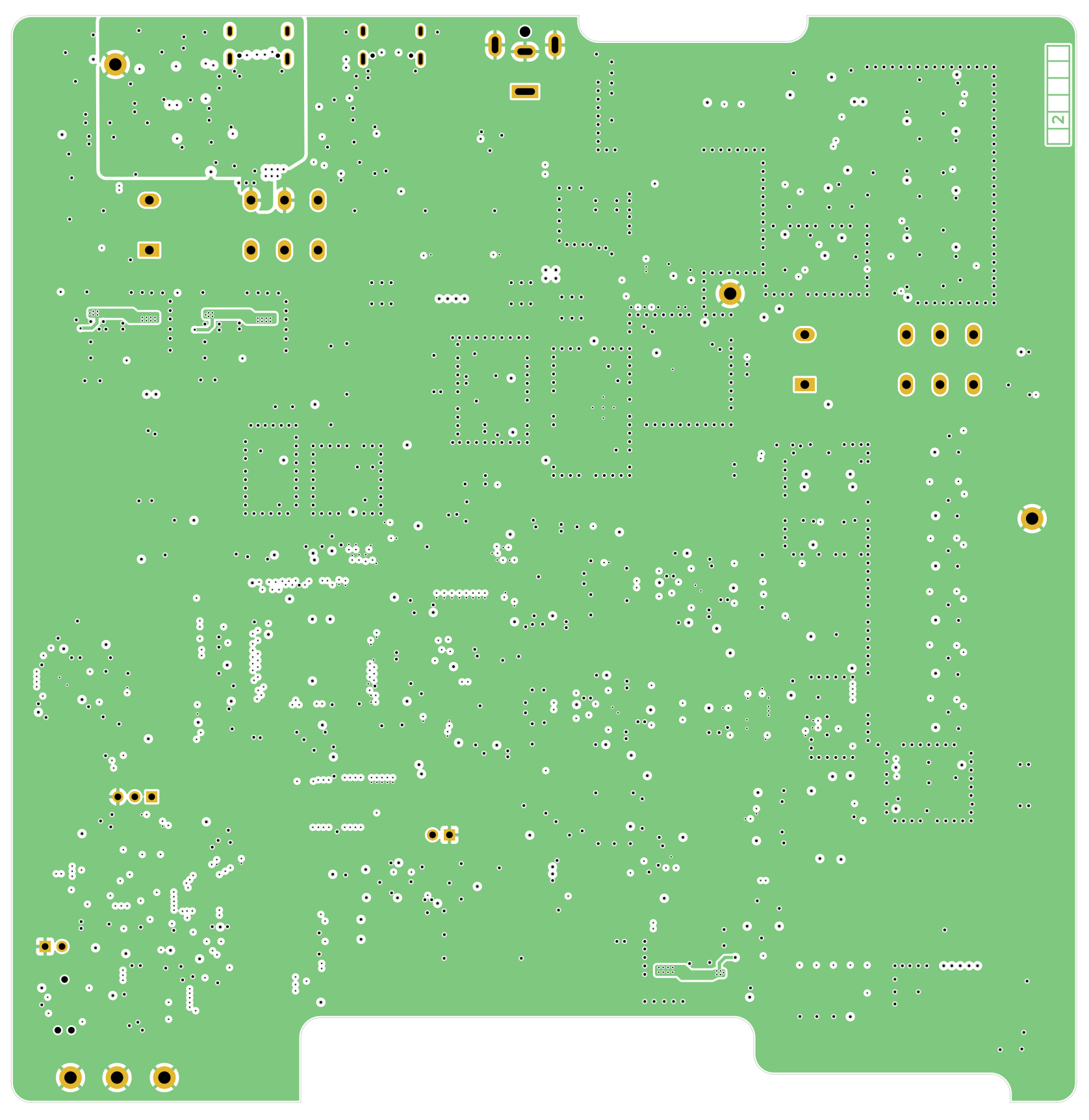
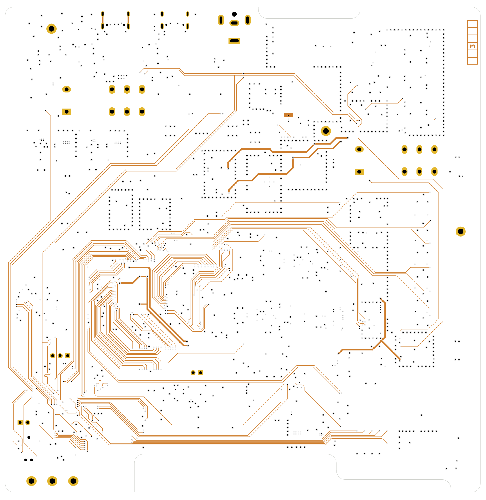
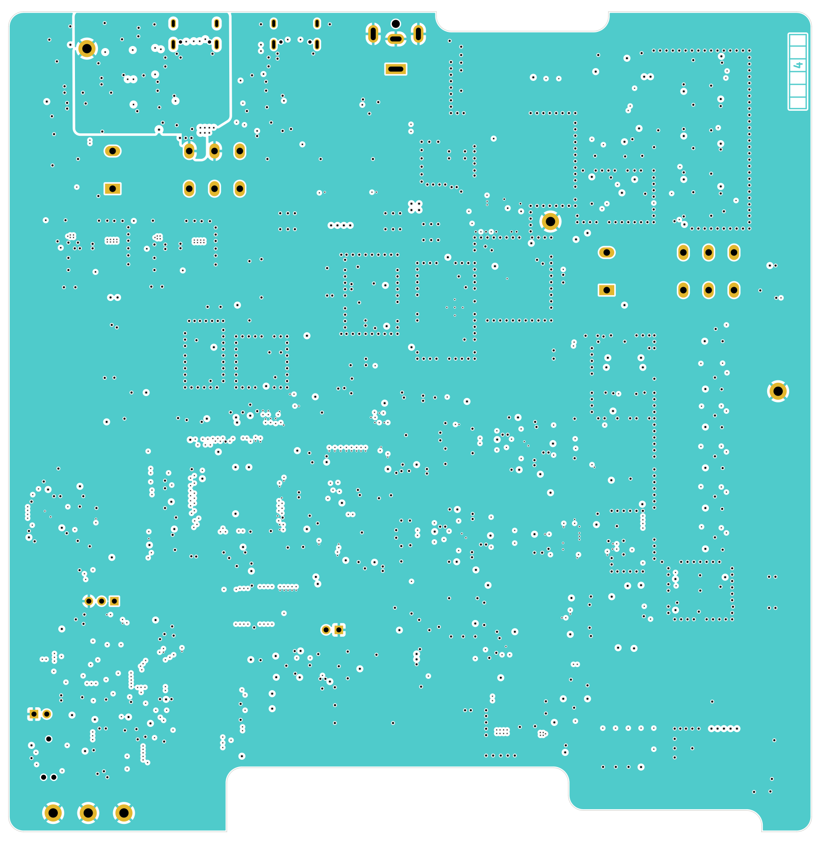
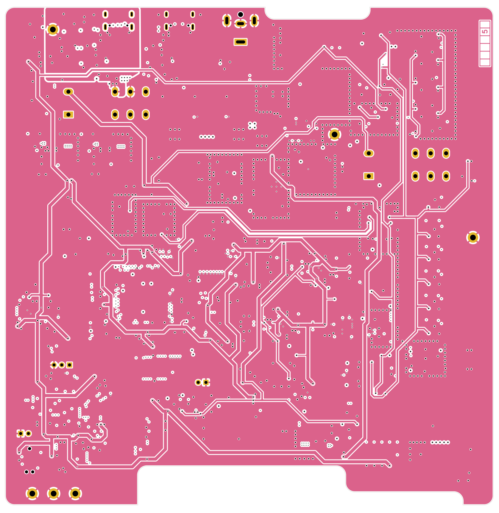
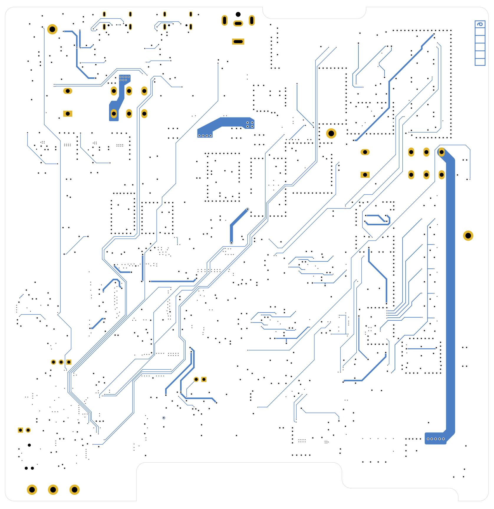
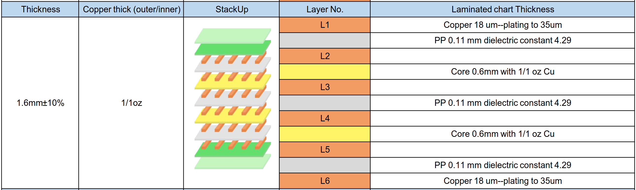
Even though everything theoretically could fit into 4-layers (I was using 4 layers almost until the end and until I started routing power tracks) the signal integrity wouldn't be that good and many of the higher speed traces wouldn't have the nice ground return path. With six layers pretty much all of the traces have a continuous ground plane in the adjacent layer.
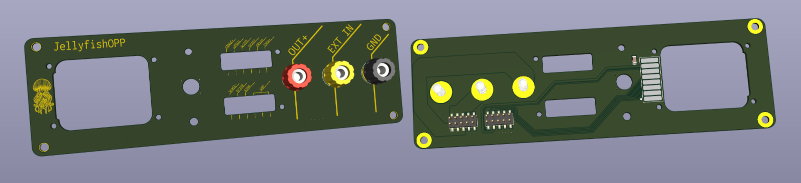
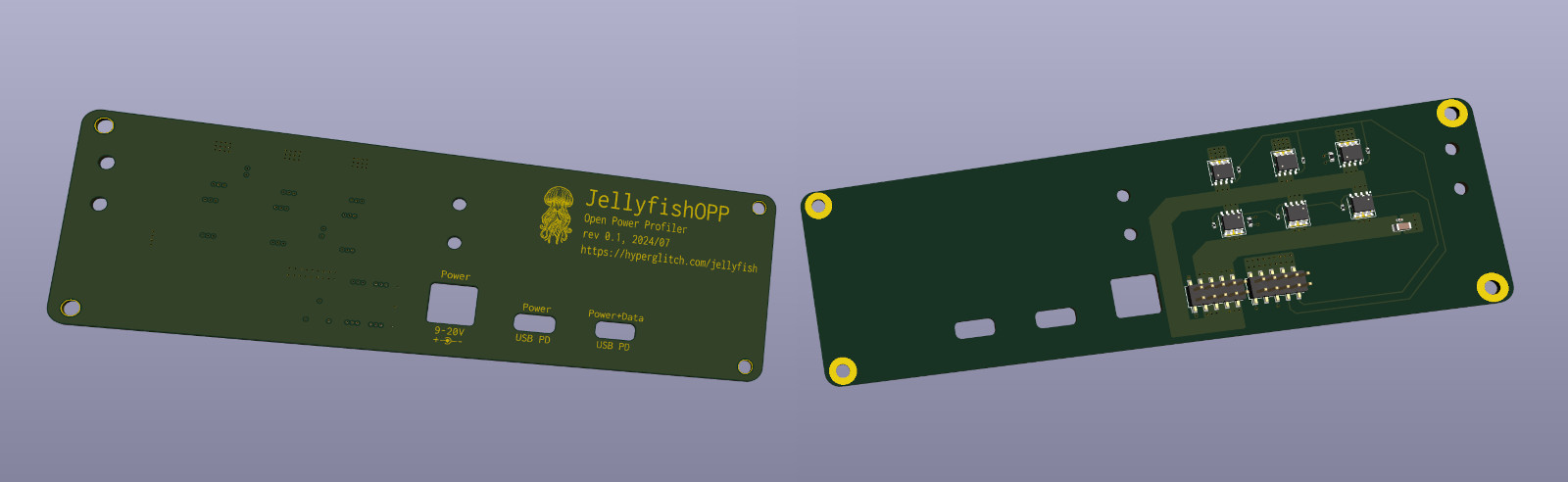
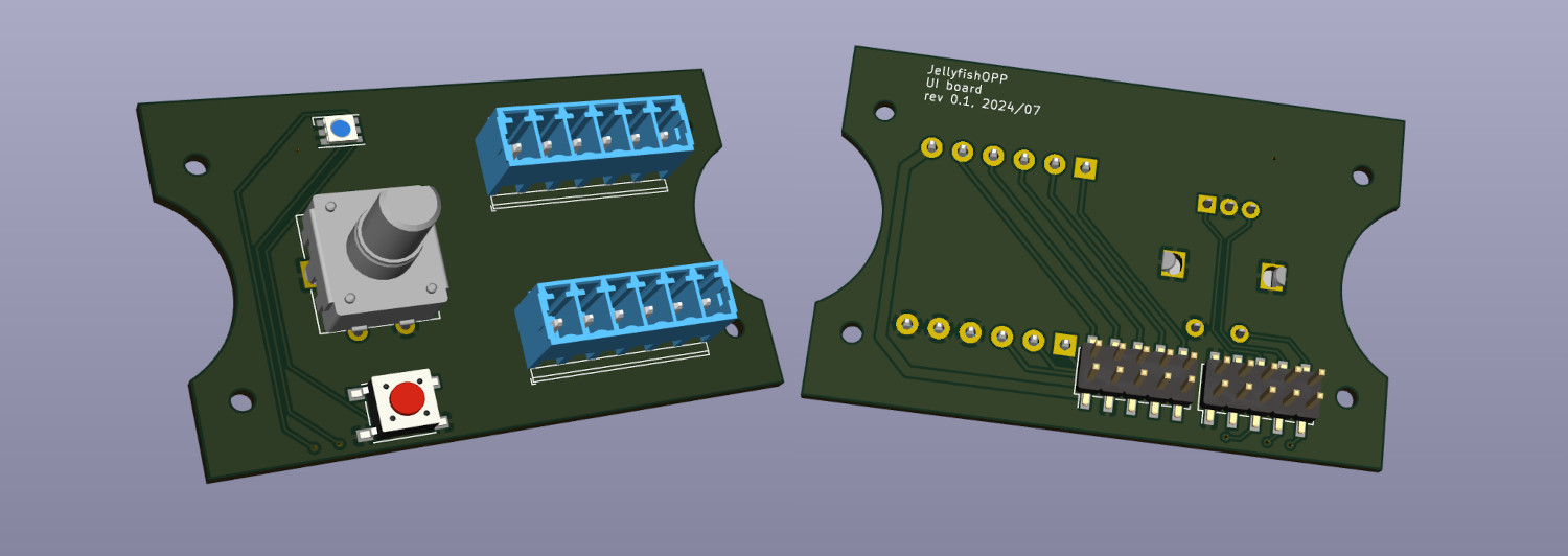
Other PCBs
Besides the main board, there are three other PCBs: front panel, back panel and UI support PCB. Front and UI boards are 2-layer boards with just a few components and back panel is 4-layer (to avoid traces on the back side) and it contains the output stage MOSFETs.
Main board preparation
KiKit is used to separate all the boards into separate files and to generate the Gerber files. After separatingg the boards I manually exported the required production files for the boards.
The main board in total contains 780 SMD components and 10 THT ones with 91 unique parts overall.
Price/Assembly/Order
After finishing the schematic I feared that the, due to everything I threw on the PCB, BOM cost would be really high. In the end, after finalizing the BOM, while it is quite high, it's actually a bit lower than I initially expected. The cost of the BOM, if ordered directly from Mouser, was about 300€ for one device or around 230€ for 10 pieces (all without VAT). There's a lot of space for improvement here but the idea is to start testing with this to get some "ground zero" results before doing further optimizations (I already added some possible optimizations to be tested, for example a MUX on ADC input which can remove the need for second ADC).
Even though I really wanted to produce the PCBs in Europe, pricewise it was just too expensive. First few quotes I got were around 4k€+VAT for one board, with lead times of 5+ weeks, which is way too much. Eurocircuits really was a nice surprise here as their total price for assmbly and components of this board was around 1700€ and, based on few previous orders, they really do great work. Aisler unfortunately doesn't produce 6-layer boards any more (although I'm not sure I would go with them as, even though I really wanted to like them and gave them a few chances, every time there were some issues, delays and unresponsiveness from their side). But the quality of their work is great.
I also got two quotes from fab houses from China. PCBWay quoted $1200 and 30 days lead time and PCBgogo quoted $950 (shipping included) with 17 days lead time. JLCPCB has really good price for 6-layer PCBs but their assembly service is mainly for use with their own stock - although is possible to order external components, with this number of components the total price would probably be quite high.
In the end I decided to go with PCBgogo. I haven't used them before but based on their social media posts I'm pretty sure it will be ok.
For the other three PCBs (front and back panel, UI support) I will go with JLCPCB and do the assembly myself as those are quite simple boards with just a few components.
Files
All of the files are available in the GitLab repository and can be downloaded from there.