
This article will specify all parts of the JellyfishOPP device. The initial schematic, followed by the PCB design, will be developed in accordance with this specification (subject to future modifications if necessary). This document is the result of research, simulations and evaluation of various development boards.
JellyfishOPP is an open source, open hardware, programmable power supply and measurement device. The main page containing the description and links to all of the development updates can be found here: https://hyperglitch.com/jellyfish.
Development of the device is funded by NLnet through the NGI0 Entrust Fund.
There's a lot to cover so this document is split into following sections.
Table of Contents
Block diagram and general overview
Main planned features of the JellyfishOPP device are:
- programmable power supply: -5-18V or 0-18V, 0-3A (limited to 10-15W output power and 1A with the negative voltage output)
- electronic load (limited to 5W sinking power for thermal reasons)
- precise voltage and current measurement across a few orders of magnitude (uA to A)
- current measurement bandwidth of 150-200kHz, 2-3MSps sampling rate
- on-device user interface for basic control and monitoring
- auxiliary 0-5V output, 0-500mA (or 0-1A) with just a basic low precision voltage/current monitoring and short circuit protection
- USB PD or DC input
- general purpose digital inputs (for recording events, UART and other communication protocols in sync with power measurements)
- general purpose 14 bit analog input (for recording analog signals in sync with power measurements, low-bandwidth oscilloscope)
- battery emulation and battery profiling features
JellyfishOPP device's main use case is when connected to a host computer or smartphone where it can be controlled and the data is streamed from the device to the host. Alternatively, it can operate in a standalone mode, offering a subset of functions such as a power supply/load, basic multimeter, and a low-bandwidth oscilloscope.

Power output stage
The device is designed to:
- provide an adjustable voltage at the output.
- include current limiting features.
- be capable of sinking current (operate within two or four quadrants).
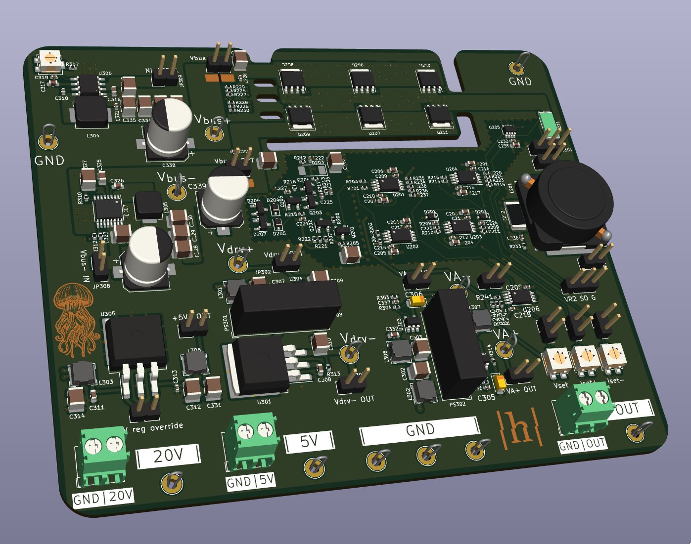
After checking out few possible options (for example using LT8714 with additional electronic load) I decided to go with a switching pre-regulator (to minimize the voltage difference) followed by a linear output stage in order to get a clean output voltage. By checking some existing projects (especially Dave Ericksson's amazing PS-Load and DIY SMU) I decided on MOSFET based complementary push-pull output stage (basically, a class AB audio amplifier) due to it's ability to provide both positive and negative output and sink the current in both polarities (four-quadrant operation). This solution does have some downsides, such as lower efficiency and thermal limitations, but provides clean output. Additionally, both positive and negative current limit are implemented in analog domain, inspired by Dave Ericksson's crossover used on few of his projects. The LTSpice simulation yielded good results so I also made a PoC board with the output stage and few power supplies to test the output stage in real life. The design files for the PoC board can be found in the main repository: https://gitlab.com/hyperglitch/jellyfish/

Given the thermal limitations of the device — a compact unit with precision analog circuitry that should keep the stable temperature to ensure accurate measurements — the output power limits will be established after further testing, likely around 10-15W for output power and 5W for sinking power.
Another downside of this type of output is risk of oscillation when handling high capacitive loads. One mitigation strategy, in addition to limiting the slew rate of the control signal, is to add inductor + resistor parallel circuit on the output which will act as high impedance for higher frequencies and reduce the oscillations. However, this additional circuit can interfere with the current limiting circuitry and the voltage control loop so some testing and adjustment will be needed.
To address thermal concerns, the output stage will incorporate multiple MOSFETs in parallel which will simplify heatsinking and cooling. Additionally, the output stage MOSFETs of the actual device will probably be placed on a separate PCB mounted on the back side of the enclosure to prevent the heat spreading to the rest of the circuitry (more details in the section about the physical form).
For precise and linear control of the output stage, especially around 0V, the MOSFET biasing circuit is required. Simulation showed good results with a circuit similar to this one.
In order for the output to come as close as possible to the power supply rails (within approximately 0.6V), the MOSFET driver power supply needs to go around 4.5V above and (a bit less) below the power supply rails (due to the MOSFET gate thresholds). That means in order to get down to 0V at the output the driver supply needs to go below GND level. Due to that, a separate (higher) voltage supply for the MOSFET driver and also a negative power rail will be added so that the device, besides the 0-18V can also give down to -5V at the output making it truly (albeit a bit limited) four-quadrant supply (negative output is limited to -5V as the used current sense amplifier has the low limit for common voltage at -5.5V). One of the considered options was also to use an integrated class AB audio amplifier as an output stage (such as TDA7293) which would simplify the design (assuming it would work) but they use only one power supply for the whole IC (without the possibility of driving the output transistors with higher voltage) so the max output voltage would be limited to 4.5V from the power rail which would be a significant drawback.
Power supplies and power routing
The device requires a lot of power rails for different parts. The main power input comes either from USB PD (Power Delivery) or from DC input jack. To accomodate situations where the host device (such as a computer or smartphone) cannot supply sufficient voltage, a secondary USB PD input (power only) is provided. Furthermore, the measurement circuitry, MCU and FPGA can be galvanically isolated from the main (data+power) USB connector. This approach allows the user to achieve a floating/isolated output when an isolated power source is used without having to add power isolation inside the device which would add to the cost and the complexity of the device. If the power from the main USB input is used then the measurement circuitry is not isolated from the USB ground.
The main power input (9-20V, or 5-20V with some limitations) is routed to different power converter blocks:
- positive tracking pre-regulator: adjustable 0V-Vin, provides the power for the positive output while minimizing the dropout voltage at the linear stage (limited to 3A)
- negative pre-regulator: fixed -5V (I'll consider adding the tracking here too), provides the negative power for the output (limited to 1A) - will probably be removed
- output driver supply: +/-24V switching regulator followed by linear regulators. Used for MOSFET drivers, low current (few dozen mA max)
- analog supply: +/-9V switching regulator followed by +/-8V linear regulation, used for powering opamps and analog circuitry, low current (few dozen mA max)
- analog 5V: clean 5V supply used for ADCs, DACs, current sense amplifiers, references, etc.
- system supply: 5V (for protections), 3.3V (for digital circuitry) and 1.2V (for FPGA)
- auxiliary power output: additional software controllable 0-5V output, 0-500mA (or 0-1A) with just a basic low precision voltage/current monitoring and short circuit protection.
Given that the dual supplies for the MOSFET driver and analog circuitry require only a low current output, small and cost-effective isolated power modules followed by linear regulators are considered. This approach will be evaluated on the PoC board and, if successful, could simplify the overall design.
2-quadrant or 4-quadrant operation
At this point, and after playing around with the PoC board, I'm more leaning towards removing the negative output voltage capability and leaving only positive source and sink options (2-quadrant operation).
4-quadrant PROS:
- more versatile
- can be used as a relatively limited SMU for testing electronic components
4-quadrant CONS:
- more complex design
- setting the output voltage to negative value by mistake can result in damage to the device under test
- more limited sink current (limited by the negative power supply)
- rarely used in practice
When sinking current, with the negative power supply present, the current return path is the negative power supply (which results in requirement to also add heatsink to it). If the negative power supply is not present, the current return path is the ground and all energy is dissipated in the output MOSFETs (which is the goal).
All-in-all, the downsides of 4-quadrant operation outweigh the benefits so the negative power supply will be removed (this only applies to the "power providing" power supply as the output driver and analog circuitry still require split power supplies). After the first prototype is done I'll consider adding this feature as an optional module.
Current/voltage measurement
Device incorporates two dual-channel ADCs:
- two channel 16-bit ADS9224, one channel is used for measuring the current in highest range, other channel is dynamically switched between measurement ranges
- two channel 14-bit ADS9234 (14 bit used as a cost reduction), one channel is used for measuring the output voltage, other channel is routed to the front panel connector as a general purpose analog input.
All channels are simultaneously sampled.
Current is measured by measuring the voltage drop across a shunt resistor. The JellyfishOPP is continuously measuring the voltage drop across two resistors: the high range one and dynamically switched one. The high range shunt resistor is also used in hardware current limiter.
Dynamically switched section consists of a three or four shunt resistor in series with MOSFETs across each enabling adding each resistor individually to the current path (resistors will be selected so that the maximum voltage drop stays below 30mV). By tracking the current value, the control circuitry (FPGA) can switch in the optimal shunt resistor in order to measure the current as precisely as possible. Based on the testing, two optional diodes (parallel, both directions) will be added in parallel to the dynamically switched section to prevent the high voltage drop in case the range switching isn't fast enough (downside is the diode leakage current which might affect the measurements in the lowest measurement range).
For shunt resistor voltage drop measurement (for both the high range and dynamically switched shunt), the INA241x bidirectional current sense amplifier is used. It comes with five available gain values, very high bandwidth, high common mode voltage and low noise. Very similar functionality (with pin-to-pin compatibility) is also available in INA296x. Both come in two versions: A with 0.01% gain error and B with 0.1% gain error (and higher offset voltage).
Sampling is done at a rate between 2 and 3 million samples per second. This allows the input signal bandwidth of 1-1.5MHz but, at least for the current signals, it will be limited (by both hardware and software filtering) to 150-200kHz. Sampling is done with FPGA to allow for lower jitter while also leaving the main MCU to handle the communication and UI.
Battery simulation
The initial idea involved integrating a voltage-controllable resistor in series with the output, which could be adjusted to accurately emulate battery behavior, such as voltage drop at a low state of charge. However, after conducting several battery measurements, it was determined that a software-controlled approach (executed by the FPGA and based on a lookup table) could yield sufficiently accurate results given the input bandwidth, while significantly simplifying the implementation. This method's effectiveness will need to be confirmed through practical verification.
Data acquisition and system architecture
Main computational elements of the device are the MCU (STMicro's STM32G4 series) and FPGA (Lattice ICE40HX1K).
MCU controls the "slow" parts of the device (hardware current limit setpoints, power routing, temperature measurement, auxiliary power supply) in addition to USB communication, user interface and fetching data from FPGA.
The FPGA (ICE40HX1K) controls the ADCs and the voltage setting DAC and performs additional digital filtering on measured values. The FPGA is also sampling the general purpose input signals in sync with the ADC measurements (these can be any sort of user provided digital signals such as UART lines, GPIOs, and others), in addition to providing the battery emulation. Depending on the performance of the initial prototype, an external SRAM memory can be added to FPGA for data buffering.
During the evaluation phase I've verified the data acquisition using the Olimex ICE40HX1K-EVB FPGA and communication between the MCU and FPGA using the Nucleo-G474RE board. The MCU and FPGA communicate over the SPI protocol which will be upgraded to QSPI in order to get faster data rates.

Physical form and connectors
Device should be easily portable and shouldn't occupy too much of the bench real-estate. The case should be made from extruded alluminum. Back side will contain the power connectors (2 x USB Type C, 1 x DC barrel jack) and heatsink (with an optional fan if needed). Front side will have a small 1.5-2" TFT screen, rotary encoder for user input, a LED for warning indication, GPIO/AUX connector (two row pluggable 3.5mm terminal block which can be used with a wide selection of terminal block plugs while also allowing a standard header pins / DuPont wires to be connected directly) and three binding posts for current input, GND and current/voltage output.
Due to the small size, the electronics will be split into three or four PCBs:
- main board with power input, PD control, power supplies, MCU, output MOSFET drivers, and others
- back panel with output MOSFETs with a heatsink (and fan if needed). This will be connected to the main board with 2.54mm header connectors. Testing will show if the MOSFETs will be placed on the inside or on the outer side of the panel (with another panel for mechanical/aesthetical reasons).
- front panel with TFT screen and cutouts for connectors and encoder
- optional analog board with current sense amplifiers, ADCs and other sensitive components. This will be needed if there's not enough space left on the main board or if the heat from the output stage spreads through the main board. It will be placed on top of the main board.
While designing the PCB, all PCBs will be laid next to each other and separated with V-cuts. This will simplify the assembly process.